Nanofabrication & Epitaxy Cluster

Forschungszentrum Jülich - Helmholtz Nano Facility (HNF)

LEED SEM FIB PVD MBE ALD Sputter Deposition SPM STM

Reference Number: 121403

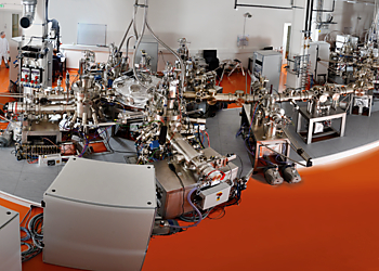
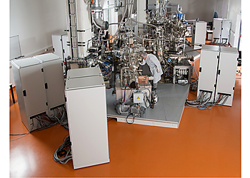
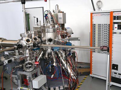
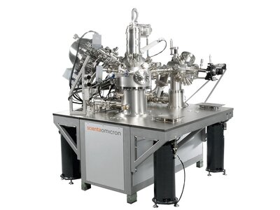
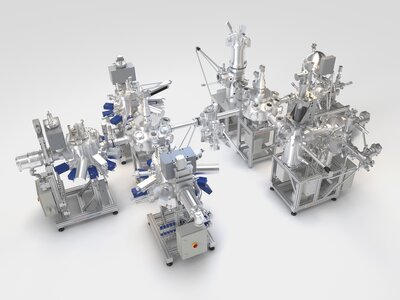
The Nanofabrication and Epitaxy Cluster is a multi-user platform of the Helmholtz Foundation for research on structures and devices for quantum computing, semiconductor technology and materials, and concepts for novel devices. Extended in 2020 by a NanoScanLab (FIB/SEM), Large Sample SPM for 4" wafers, and LEED module.

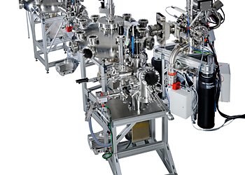
  • 14 Module UHV Cluster System for up to 4" Wafers
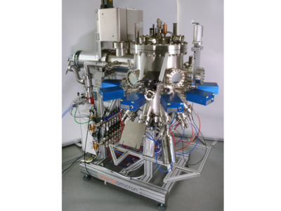
  • Four PRO 100 MBE Modules
  • Three Sputter Modules
  • Interface to 3rd Party ALD
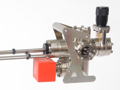
  • 2 Wafer Introduction and Preparation Modules
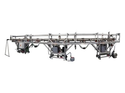
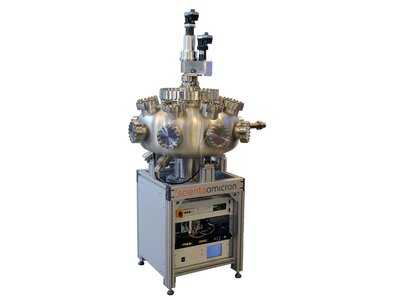
  • 2 Radial Distribution Chambers and 2 Linear Transfer Lines
  • Wafer Tracking
  • NanoScanLab (FIB/SEM)
  • Large Sample SPM for 4" wafers
  • LEED module

Integrated Instruments