Local News - Japan
Scienta Omicron ローカルニュースページへようこそ!
Following a strategic update to our operations in Japan, Scienta Omicron now serves the market through our exclusive partner, Vacuum Products Co., Ltd. This ensures continued high-quality local support, sales, and service for our customers.
For more information about our products and support in Japan, please visit Vacuum Products: Vacuum Products Inc.
Links to Product Information (in English)
Materials Innovation Platform
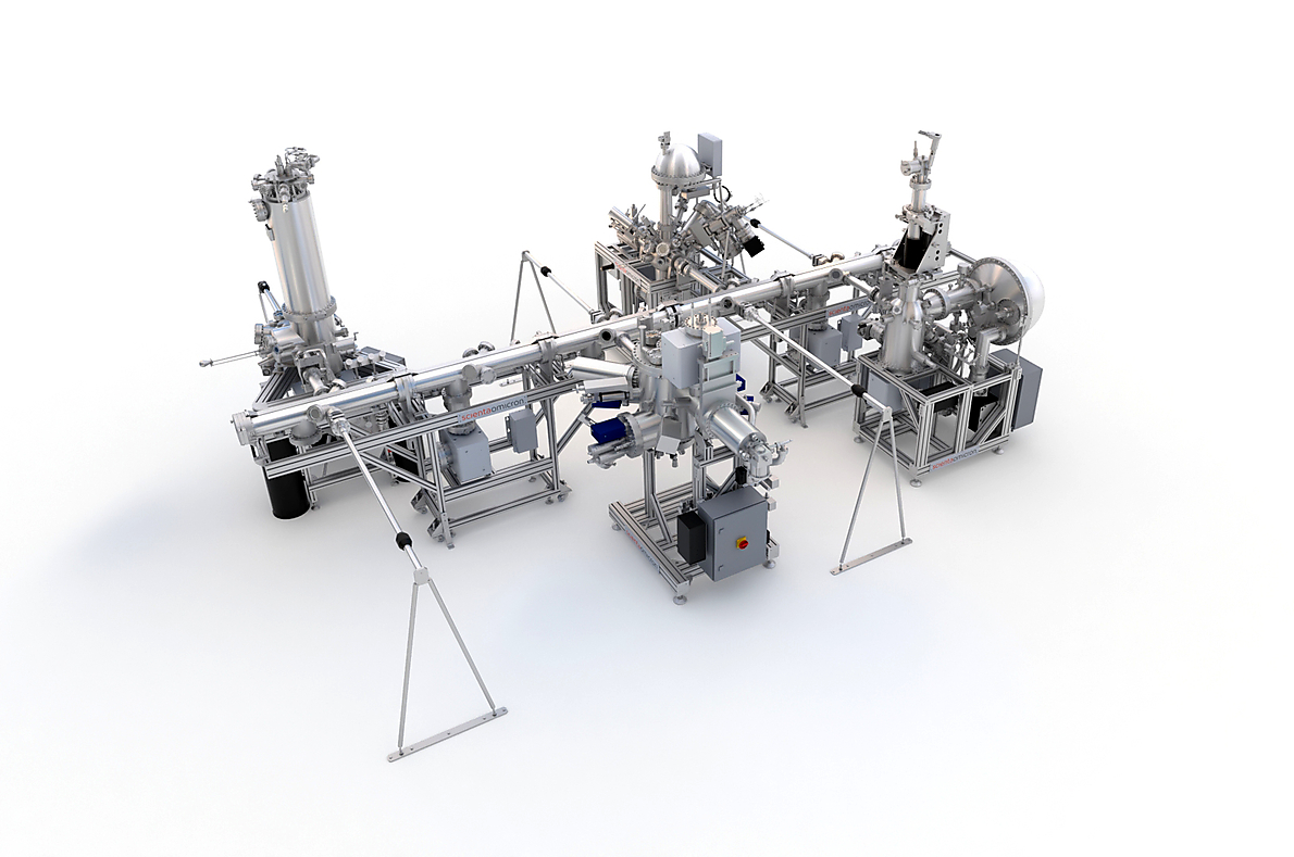
Scienta Omicron has a long history of providing customised solutions for the surface science field. Tailored instruments and large scale Materials Innovation Platforms (MIPs) offering unique capabilities is the best choice for the scientist breaking barriers in surface science techniques with extraordinary requirements.
Materials Innovation Platforms (MIPs) integrate instrumentation for growth with sophisticated in-situ characterization tools. Samples can thus be analysed at intermediate process steps to understand cause-effect correlations of a novel material’s growth and structure without leaving the clean UHV environment at any time. Scienta Omicron’s broad portfolio enables us to act as a single source supplier and a reliable partner for the design, production and in-field support, ensuring a smooth delivery process and a high system uptime.
Scanning Probe Microscopy

Our modern scanning probe microscopes offer ultimate mechanical stability, ultra-long hold times at liquid Helium temperatures, options for strong magnetic fields in a customized UHV system environment. We have carefully optimized our instruments to ensure outstanding signal qualities for QPlus and STM operation to ensure excellent results in all relevant scanning and spectroscopy modes. In addition, we have advanced controller technology enabling e.g. a new QPlus operation mode called QSPEED simplifying QPlus operation.
Our SPMs offer the most advanced techniques allowing for new experiments such as tip enhanced Raman, scanning tunneling luminescence, time resolved STM and electron spin resonance experiments enabled through adequate optical solutions or high frequency wiring.
Electron Spectroscopy

In 1983 – two years after receiving the Nobel Prize – Prof. Kai Siegbahn co-founded Scienta for the continued develoment of electron spectrometers and systems. Since the start, we have been the market leading, most innovative supplier of high-end photoelectron spectrometers.
Thin Film Deposition

Since 1998 we have focused on the increasing demands of the growth and characterisation of high-purity epitaxial layers (MBE) combined with in-situ scanning probe microscope (SPM) and electron spectroscopy (XPS, ARPES, SAM).
Scienta Omicron offers compact MBE systems for fundamental research. The available sample size ranges from flag style samples up to 4” wafer samples.