

Materials Innovation Platform (MIP)
Accelerating the Pace of Discovery
PVD MBE Laser MBE ALD Sputter Deposition DC Sputter Deposition RF Sputter Deposition EBPVD CVD PE CVD
- Multiple deposition modules and/or different deposition technologies
- Surface analysis between process steps for chemical, electronical and structural investigation
- Ultra-clean UHV environment at any time during the transfer between modules
- Leading scientific components for forefront research
- Largest installed base
- Extendability for additional deposition or analysis techniques
The Materials Innovation Platform (MIP) integrate instrumentation for growth with sophisticated in-situ characterisation tools. Samples can thus be analysed at intermediate process steps to understand cause-effect correlations of a novel material’s growth and structure without leaving the clean UHV environment at any time. Scienta Omicron’s broad portfolio enables us to act as a single source supplier and a reliable partner during design, production and in-field support, ensuring a smooth delivery process and a high system uptime.
Novel materials with unique properties are key enablers for new, disruptive technologies. Of special interest are nanomaterials, which can be engineered for specific physical, electrical, and chemical properties by exploitation of quantum size effects. Understanding cause-effect correlations of these materials' growth and structure supports the systematic discovery and optimisation of the desired properties. A proven and effective approach for this research is to use a 'Materials Innovation Platform'.
Materials Innovation Platforms (MIP) integrate instrumentation for growth and detailed characterisation of samples in-situ. Not only is sample quality preserved by maintaining UHV conditions, but analysis and growth can be done at intermediate process steps and performed far more rapidly than if the instrumentation was separated. Further, appropriate design of a MIP provides for expansion and exchange of capabilities as the research evolves. Working with a single supplier and partner to design, produce and support these MIPs ensures highest instrument uptime, ease-of-use, and productivity.
Enabling Forefront Research
Modern application fields need both, a fundamental understanding of the underlying physics and chemistry, as well as an integrated approach towards device implementation. A Materials Innovation Platform is the key to success whenever one of these topics is required:
- Multiple deposition modules and/or different deposition technologies
- Ultra-clean UHV environment during transfer between modules at any time
- Surface analysis between process steps for the chemical, electronical and structural investigation of surfaces and interfaces
- Extendability for additional deposition or analysis techniques
More Information
MIP Core Competencies
Our core competencies enable your success in challenging multi-module projects.
Competence
- Tailoring solutions to the scientific needs (more than 1000 UHV systems delivered)
- Single source supplier and full project responsibility
- Global sales & service organisation
Application Know-How
- Technology leader in UHV surface analysis & MBE
- More than 30 supported technologies
- Experience in identifying suitable analysis techniques
Modular, Configurable & Extendable
- Installed base: > 20 complex MIPs, rapidly growing
- Quality & reliability ensures highest up-time
- Configurable modules for easy integration
Technical building blocks
- High quality UHV solutions
- Linear transfer (LTL)
- Radial distribution (RDC)
- Mistral system control
- Special purpose modules
Surface Analysis Techniques
Scienta Omicron offers the broadest range of UHV surface chemical and structural analysis techniques, fully integrated and interfaced by a single supplier. Virtually any of our turn-key analysis systems is suitable for use within a Materials Innovation Platform. Third Party systems such as Atomic Layer Deposition (ALD), Focused Ion Beam Lithography (FIB) and many more can be interfaced using dedicated buffer and sample handling systems.
- Angle Resolved Photoemission Spectroscopy (ARPES Lab)
- X-Ray Photoemission Spectroscopy (XPS Lab)
- Hard X-Ray Photoemission Spectroscopy (HAXPES Lab)
- Momentum Microscopy (NanoESCA)
- Scanning Auger Microscopy (SAM)
- Scanning Electron Microscopy (UHV-SEM)
- Scanning Probe Microscopy (SPM), at variable and low temperatures, and in high magnetic fields
- Atomically precise electrical probing (LT Nanoprobe)
Thin Film Deposition Techniques
Proven research MBE systems - easy to use, flexible, expandable, and covering the full range of MBE-based technologies from small sample plates up to 4" wafers.
- Si/Ge, III-V, II-VI
- Oxide, Nitride
- Organic MBE
- Transition metal dichalcogenides (TMDs)
- Topological insulators
- Laser MBE
Interface technologies for Atomic Layer Deposition (ALD), Pulsed Laser Deposition (PLD), Sputtering and more...
Reference Systems

 with MBE and Surface Analysis")
 | © Penn State University")

, Atomic Layer Deposition (ALD), and in-situ X-Ray Photoelectron Spectroscopy Laboratory | © Scienta Omicron")


 System and Angle-Resolved Photoemission Spectroscopy (ARPES) Cluster Tool for the Nanyang Technological University | © Scienta Omicron")


Downloads
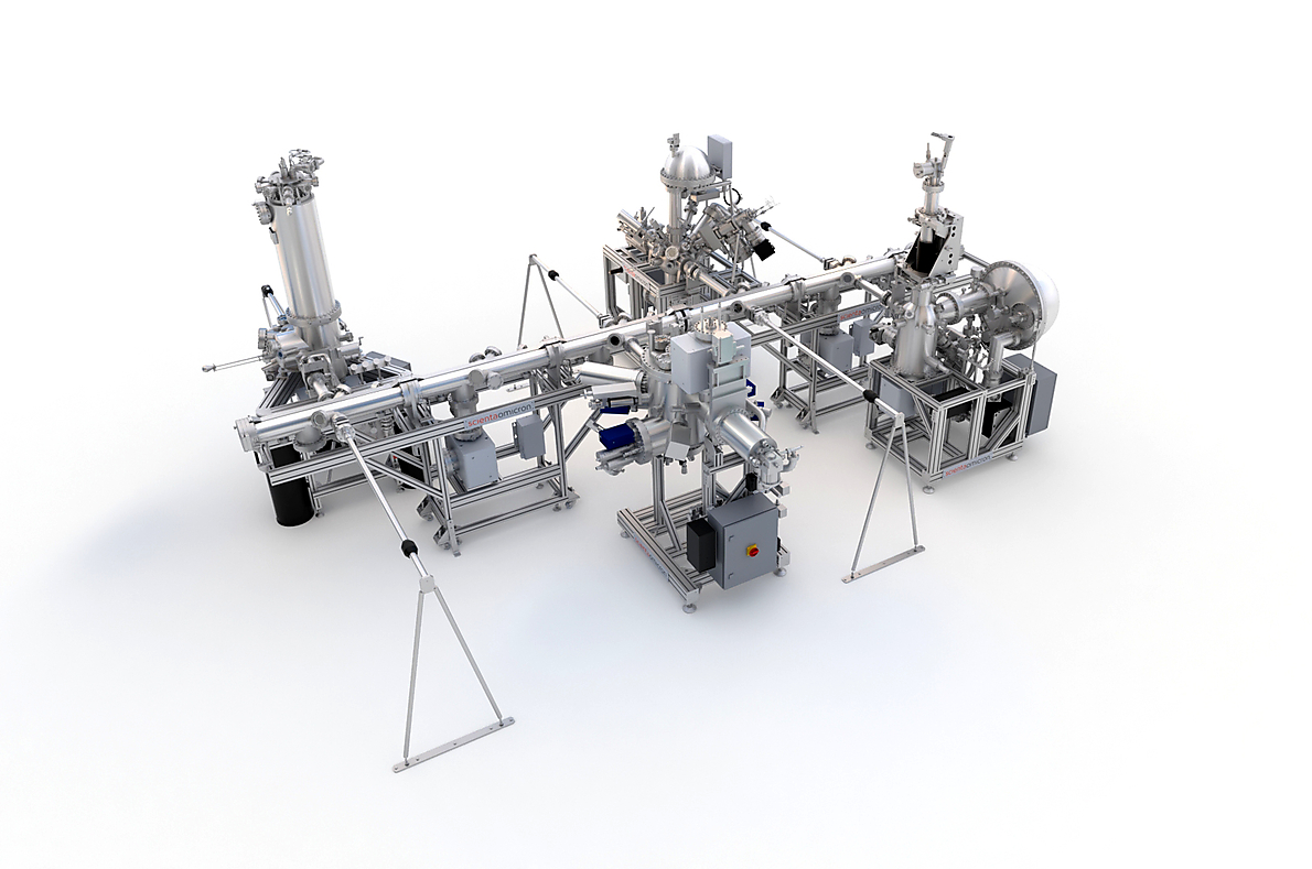
APPES/XPS MIP system in Japan
A APPES/XPS MIP system for catalyst research was successfully installed at the National Institute for Material Science (NIMS) in Japan at the end of March 2023.