Scientific Results
The Scientific Results are written by both internal and external scientists based on remarkable and interesting results and measurements done by Scienta Omicron systems and instruments. These Results offer product specifications, in-depth analysis and added information on measurements and instruments. Also, references to publications or Scienta Omicron users for further reading or information is found to promote papers and networking in the scientific community.
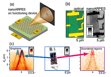
nanoARPES on Functioning and Tunable Devices with a DA30-L
In their recent paper, A. J. H. Jones and S. Ulstrup et al. explore engineering properties of quantum materials by placing a singularity of the density of states near the Fermi energy. Using ebeam lithography for structuring and formation of electrical contacts, a device consisting of twisted bilayer graphene (twBG) on a stack of hBN and graphite was formed. The device was wire bonded to a chip package and introduced to the nanoARPES branch of the I05 beamline at the Diamond light source.
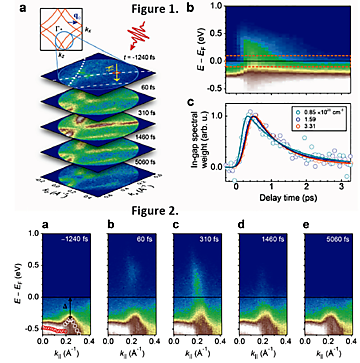
Time Resolved Photoinduced Phase Transitions in LaTe3 with an ARTOF Analyser
A. Zong and N. Gedik et al. investigated photoinduced phase transitions in LaTe3 with their time resolved (tr) ARPES setup using an ARTOF analyser. With the pump-probe scheme and a controlled time delay between photon pulses, tr-ARPES allows the generation of non-equilibrium states and track the dynamics in momentum and energy-resolved fashion.
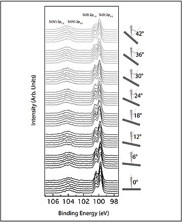
AR-XPS at Environmental Conditions
Angle-resolved x-ray photoelectron spectroscopy (AR-XPS) can be used for non-destructive sample depth profiling. Here we demonstrate the power of this technique for determination of thicknesses of thin films with sub-nanometer resolution under high vacuum (HV) conditions as well as under environmentally relevant conditions (0.1 Torr). The experiments where performed on native silicon oxide using a differentially pumped Scienta Omicron R3000 HP analyser and a high pressure adapted Scienta Omicron MX650 monochromated aluminium K α x-ray source, at the Philadelphia environmental XPS (E-XPS) system. The data are presented in Review of Scientific instruments (F. Mangolini, 83 (2012) 093112)
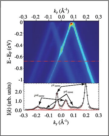
ARPES on Nearly Ideal Graphene
In the chase of new materials suitable for nano-electronics etc. great interest is paid to graphene. Ideal graphene is a pure two dimensional sheet of carbon that has a two-dimensional isotropic liner dispersion of the π and π* bands near the Dirac point such that it defines a cone with an apex at the Dirac point of energy. M. Sprinkle et al. used angular resolved photoelectron spectroscopy (ARPES) in there study presented in PRL 103 (2009) 226803 for a first direct observation of a nearly ideal graphene band structure. The observations was made on graphene grown on the SiC(000-1) surface using Scienta R4000 and SES 100 analysers located at the Cassiopée beam line at SOLEIL and at the 12.0.1 beam line at the Advanced Light Source (ALS).
LT STM: Atomic-scale Rewritable Memory Using Scanning Tunnelling Microscopy Techniques
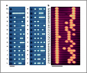
Prof. Wolkow and his co-workers at the University of Alberta in Edmonton, Canada have created the most dense, solid-state memory in history using scanning probe microscopy techniques.
Au(111) Surface State - Measured in Less Than a Minute
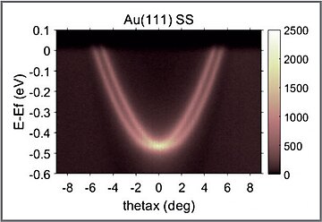
The Deflection mode patent pending Scienta Omicron DA30-L analyser is demonstrated for the case of Au(111). The data presented is recorded in less than a minute at Elettra, BL 9.2 – APE.
Au(111) with DA30-L Deflection Mode and VUV5k
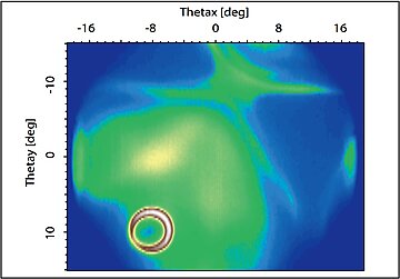
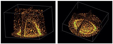
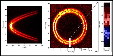
As proof of performance and as part of the characterization of their new DA30-L and VUV5k ARPES system the Prof Bing Wang group of University of Science and Technology of China have measured a Au(111) sample. The data shows a well resolved surface Shockley state with the characteristic spin split parabola. Using the DA30-L deflection mode a full data set was acquired without rotation of the sample. This is illustrated by the graph showing a series of parallel kx-ky cuts in momentum space.
High resolution 3D spin-ARPES with DA30-L and VLEED and VUV5k
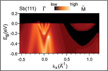
In this application note we show results from a high resolution Spin-ARPES experiment of Bi(111) using the DA30-L with a 3D VLEED type detector and a VUV5k by Yaji et al., Review of Scientific Instruments 87, 053111 (2016), (https://doi.org/10.1063/1.4948738).
Large Rashba Effect Observed with Scienta Omicron ARTOF 10k
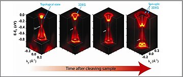
The field of spintronics deals with ideal devices which can operate using the electron’s spin, rather than its charge. A new class of materials, called topological insulators, is intensively studied in the past years. Their unusual property is that the surface behaves as a metal, whereas its bulk structure has a semiconductor behaviour.
Laser ARPES with ARTOF 10k
In ordinary insulators such as diamond the occupied and unoccupied electronic states are separated by a large energy gap. This gap prevents current flow when an electric field is applied. In topological insulators however, electrons can bypass the energy gap by moving in surface states. This new class of materials exhibit unusual properties which may be important for quantum computing.
Laser ARPES with R4000
In this application note the high-energy electron dynamics in Bi2Sr2CaCu2O8 high temperature superconductor has been studied by laser-based angle-resolved photoemission.
nanoARPES or k-Microscope
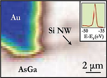
In nanotechnology and nanoscience the objects are in the order of 10-9 m. The properties are known to be different for a material in the nano-meter size compared to bulk. An important factor to understand and control these property changes is to gain insight in the electronic properties of the material, not only with high resolution in energy, angle and reciprocal space, but also with high lateral resolution. Photoelectron spectroscopy is a perfect tool for electron property studies; with x-ray photoelectron spectroscopy (XPS) it is possible to study the core levels of a material and acquire element specific chemical information and with angular resolved photoelectron spectroscopy (ARPES) it is possible to map the band structure of a material. In order to make use of XPS and ARPES in nanoscience Maria Carmen Asensio et al. have developed a new technique where the light is focused down to nanometre size – defining the area studied with photoelectron spectroscopy (PES) to be in the nano meter size.
Observation of Topological Superconductivity on the Surface of an Iron-Based Superconductor
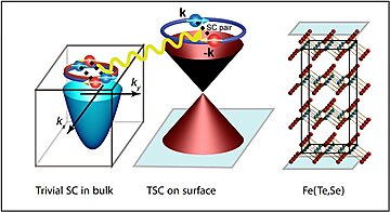
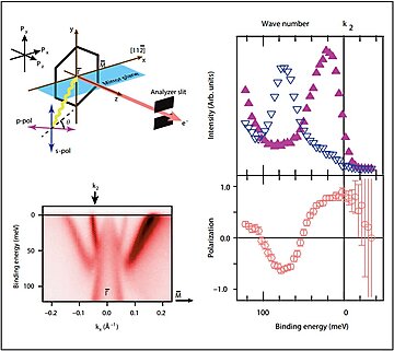
Topological superconductors are predicted to host exotic Majorana states that obey non-Abelian statistics and can be used to implement a topological quantum computer. By using high-resolution spin-resolved and angle-resolved photoelectron spectroscopy, P. Zhang et al., Science 10.1126/science.aan4596 (2018), are likely the first to show that the surface states of FeTe0.55Se0.45 are 2D topologically superconducting. The result is illustrated in Figure 1.
Plasmaronic Particles in Graphene
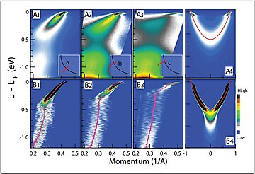
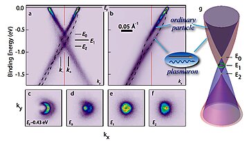
Graphene have rendered a huge interest over the last years due to its promising future in a variety of fields, such as in electronic applications where it is a candidate for ‘post-silicon’ transistors. But it also offers new insights in physics. A. Bostwick et al. report in Science 328(2010)999 on the first observation of plasmaron bands in any material as detected in graphene using angular resolved photoemission (ARPES) offers new insights in physics. A. Bostwick et al. report in Science 328(2010)999 on the first observation of plasmaron bands in any material as detected in graphene using angular resolved photoemission (ARPES).
Probing Bulk Band Structure using ARPES
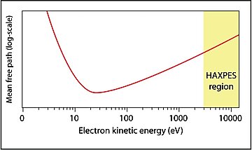
Traditionally, angular resolved photoemission (ARPES) is used to study the band structure of materials. The photon range used normally makes the technique surface sensitive. In order to increase the bulk sensitivity of the technique, ARPES spectra could be acquired using higher excitation energies. As the energies are increased the demands of the analyser, in terms of energy and angular resolution, is increasing. In this application note we present data from Chuck Fadley and co-workers, recorded using VG Scienta hemispherical analysers, showing band structure for > 1keV kinetic energies and true hard x-ray (HAX) angular resolved spectra at 6 KeV: data that have revolutionized the method of ARPES as it now allows probing the true bulk band character of a material.
QPlus AFM on NaCl (001) at Low Oscillation Amplitudes using Matrix 4 AFM PLL with TipGuard
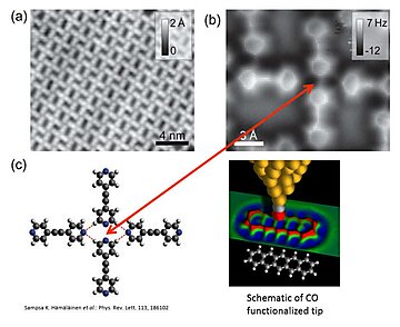
The improved QPlus AFM sensors is equipped with 1) the newest generation of Giessibl sensors; 2) integrated electrodes; 3) new high precision manufacturing; 4) higher Q-factor ≈ 90.000 at T=5K; and 5) better reliability.
Spin-Dependent Quantum Interference Studied with DA30-L & VLEED Laser-ARPES
In the paper Spin-dependent quantum interference in photoemission process from spin-orbit coupled states, Nature Communications 8, 14588 (2017), doi:10.1038/ncomms14588, Koichiro Yaji et al. show how laser based spin- and angle-resolved photoelectron spectroscopy is used to study the spin-orbital texture, and especially three-dimensional spin-rotation effects, in a surface state of Bi(111).
Spin-Resolved ARPES of Au(111) with DA30-L, 2D Ferrum VLEED and VUV5k
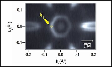
Prof. Lin of the Natioal Tsing Hua University has a Spin-ARPES system based on the Scienta Omicron DA30-L analyser with a 2D Ferrum VLEED spin detector and the VUV5k UV source. Test measurements were made using a cooled Au(111) sample.
Topological Insulators
“Not since the isolation of graphene has a new material generated as much excitement among physicists as the discovery of topological insulators.” Highlights in Nature vol 6 2010. A topological insulator is as an insulator that has a metallic boundary when placed next to a vacuum or an ordinary insulator (See for example J. E. Moore, Nature 464(2010)08916.) These exotic materials can possibly be used in technological applications such as spintronics and quantum computing.
Ultra High Resolution Photoelectron Spectroscopy
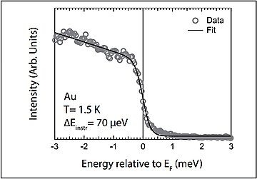
Photoemission (PES) has the ability to detect very small features in the band structure crucial for understanding the function of e.g. superconductivity, where it is of utter importance to determine the gap symmetry and positions of the nodes. This is illustrated by a study of the KFe2As2 iron-pniptide superconductor presented by K. Okazaki et al. in Science 337 (2012) 131. The data is recorded using a state of the art setup at Professor Shin’s lab at the Institute of Solid State Physics, University of Tokyo, including a Scienta Omicron R8000 hemispherical analyser, an upright helium-impounding cryostat and a laser system. This setup holds the world record in instrumental resolution of 70 μeV.
Valence Band Spectroscopy Using VUV5000
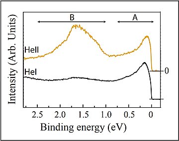
The change in line shape and peak positions of valence band photoemission (PES) spectra due to change in excitation energy can be attributed to cross sections. This fact can be used in valence band studies to assign features to specific element and orbital configurations, as done by the group of Professor Maiti, using HeI (21.2 eV) and HeII (40.8 eV) light for determining the valence band composition of the EuFe2As2 compound.
