NanoScan Lab
A Versatile Tool for Surface Analysis on the Nanoscale
SEM SEMPA EDX EBID EBIC FIB EBL
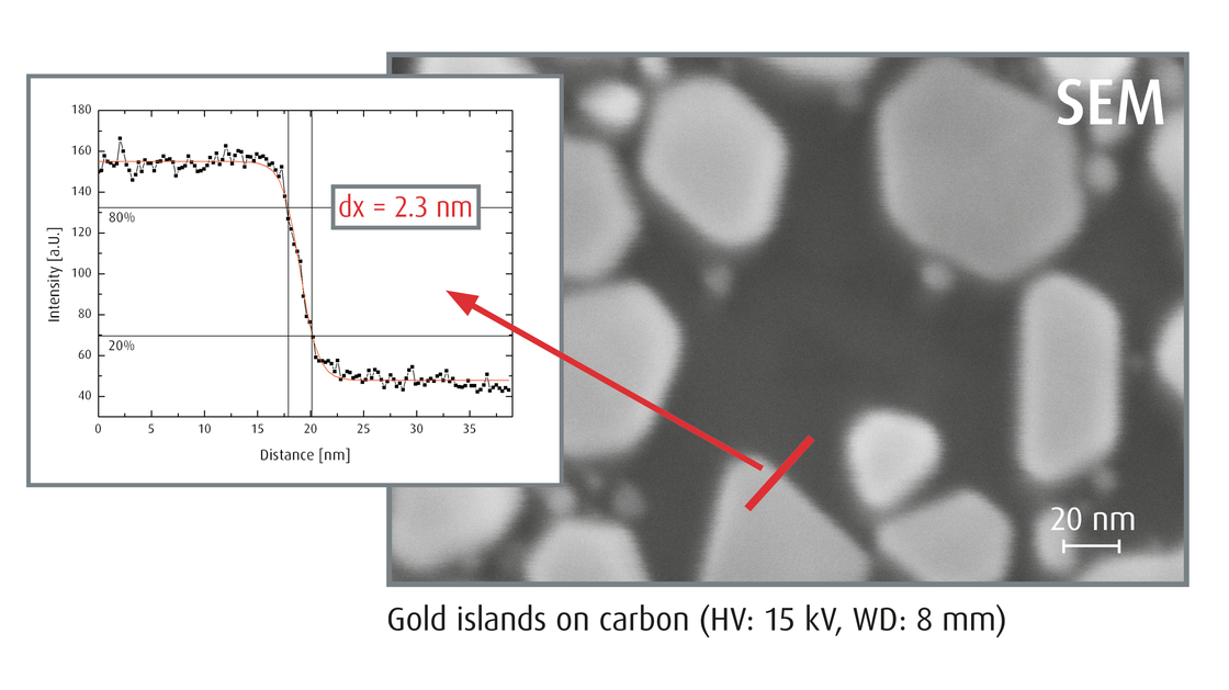
- UHV-Gemini SEM column with superb spatial resolution (achieved: SEM < 3 nm) and additional optimisation for high currents Auger electron microscopy at low beam energies high currents
- Wide range of analysis techniques, including SEM with Polarization Analysis (SEMPA), Focussed Ion Beam milling (FIB), and many others
- High-stability 4-axis sample stage for Scienta Omicron’s flag-style sample holders with a maximum tilt angle of ± 60° and optional LHe cooling to < 30 K
- Integration with other Scienta Omicron system modules allows customers to get a solution tailored to their needs
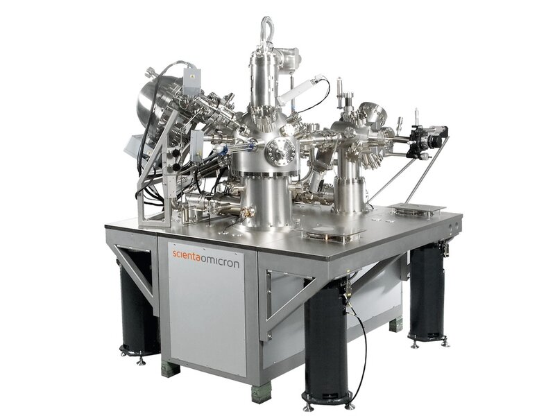
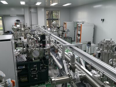
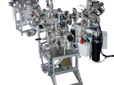
The NanoScan Lab is a versatile tool for surface analysis on the nanoscale. Based on a UHV-version of Zeiss’ Gemini SEM column, there is a wide range of options, such as SEM with Polarization Analysis (SEMPA), focussed ion beam milling (FIB), cathodoluminescence (CL), e-beam lithography (EBL), electron-beam induced deposition (EBID), and energy-dispersive X-ray spectroscopy (EDX).
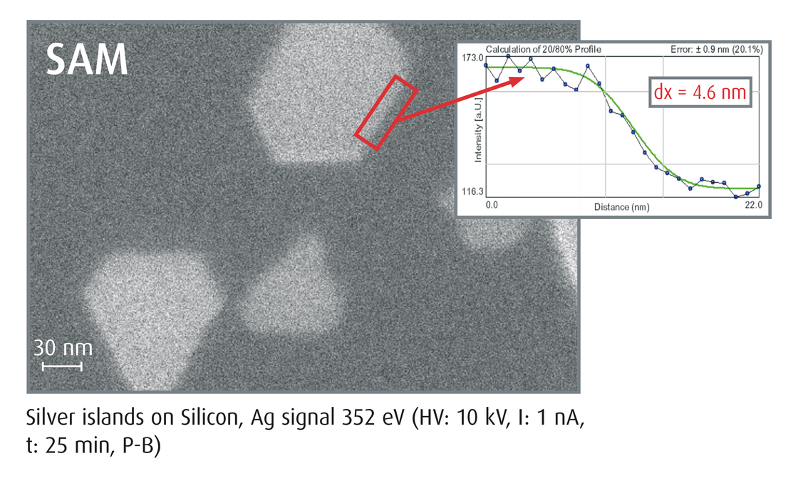
The NanoScan Lab is the ultimate tool for the analysis of small structures. Driven by the unique performance of the UHV Gemini electron column, it guarantees unrivalled resolution below 6 nm in Scanning Auger Microscopy (SAM) and better than 3 nm in SEM.
In contrast to other Auger tools, the extremely good resolution is not only available at standard 20 keV beam energy, but even at 5 keV the SAM resolution remains below 10 nm. This allows operation in a parameter range where the Auger cross sections are high and well documented for quantitative analysis.
The NanoScan Lab is tailored for the fast and efficient acquisition of data on routine samples, while maintaining the flexibility to operate in untypical parameter ranges on challenging materials. Furthermore, the NanoScan Lab may be extended with additional, complementary techniques, for example, depth profiling or SEM with Polarization Analysis (SEMPA) to get access to the magnetic domain structure. Other available methods for the NanoScan Lab include focussed ion beam milling (FIB), X-ray photoelectron spectroscopy (XPS), electron beam lithography (EBL), energy-dispersive X-ray spectroscopy (EDX), electron beam induced deposition (EBID) and cathodoluminescence (CL).
More Information
UHV Gemini
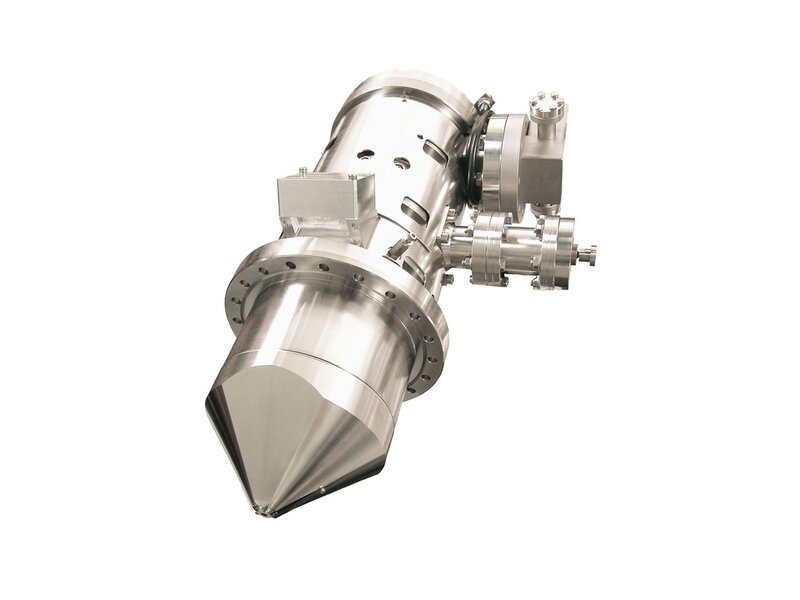
The patented UHV Gemini SEM column is the electron source with the highest resolution available for UHV operation. Designed for true UHV (< 1x10 -10 mbar), the column is fully bakeable up to 180 °C and operates without any measurable outgassing – a must for contamination-free research on many materials.
The design of the UHV Gemini is the result of a collaboration between Scienta Omicron, CEOS and Carl Zeiss NTS, employing the same electron optics as used in the Zeiss Gemini SEM product range. The Gemini column is controlled by a versatile state-of-the-art SEM electronics package from German specialist point electronic.
Besides the integrated in-lens secondary electron detector, which grants optimal detection efficiency, the UHV version offers special features that make it especially suitable for experiments using low-energy electrons and high beam currents, e.g. to image magnetic domains in SEM with polarization analysis (SEMPA).
4-Axis Sample Stage
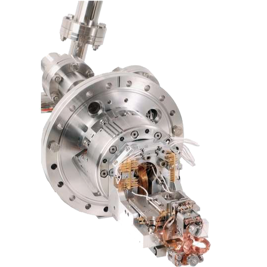
Ultimate SEM resolution can only be achieved with a highly stable sample stage. The sample stage used for the NanoScan Lab is mounted on an ex vacuo goniometer and an x/y/z stage with a travel range of 10 mm for all three axes. Due to the compact shape of the sample stage, the sample normal can be tilted by up to ± 60° with respect to the SEM axis. (Please note that the exact limits depend on the configuration with analytical components.)
The stage is designed for Scienta Omicron’s flag-style sample holders with a size of approximately 15 x 18 mm². A combination of a NanoScan module with any other Scienta Omicron module, e.g. MBE or ARPES, therefore offers the pathway to tailor a solution exactly to the customer’s needs.
The stage is equipped with a radiative heater element that allows sample heating from room temperature to 750 K. LHe cooling is optionally available and extends the accessible temperature range down to well below 40 K.
Electrical sample contacts and other customizations are available on request.
High magnification Auger measurements make great demands on the mechanical stability of the sample stage. Based on Scienta Omicron´s SPM expertise, the 4-axis sample stage represents an extremely stable and low drift platform with a non-magnetic UHV drive technology.
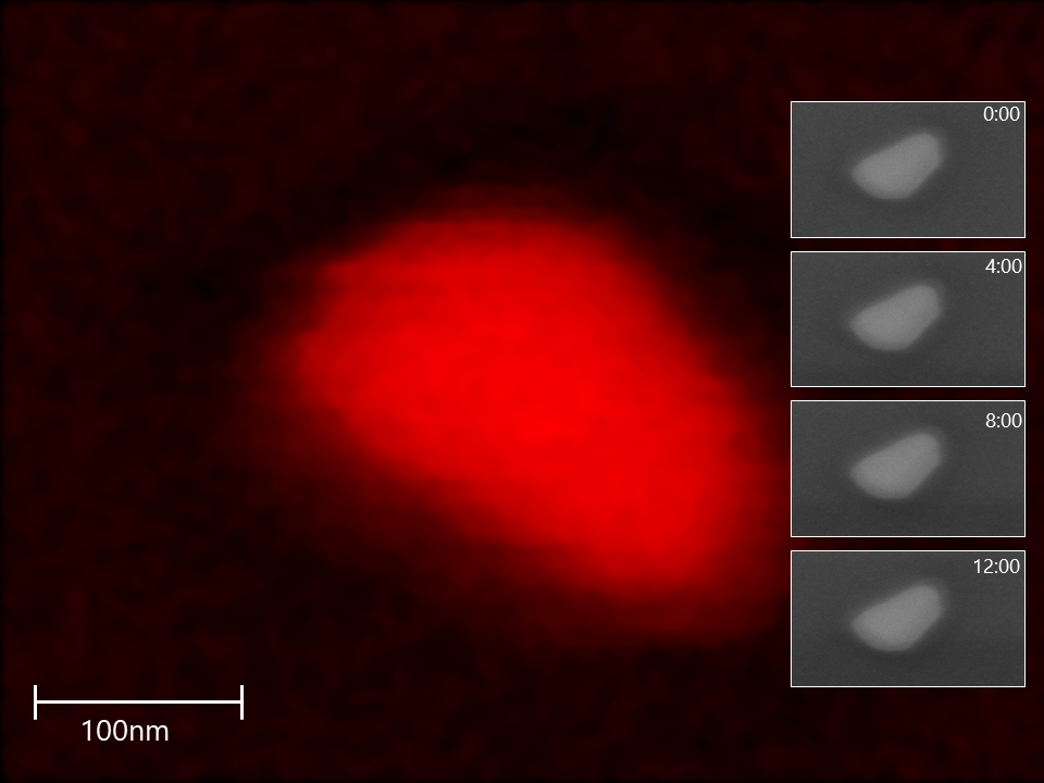
Measurement times in Scanning Auger microscopy can easily exceed several minutes - in the case of elemental maps even hours. A technically mature electronic drift correction is therefore indispensable to access a suitable performance level at small structures or at very low elemental concentrations. Based on the conventional approach employing image correlation of sequential SEM images and step-wise correction of the electron beam position, the new Dynamic Drift Correction minimises the effects of thermal and mechanical drift.
This combination of careful mechanical design and Dynamic Drift Correction provides outstanding drift values below 10 nm vectorial shift per 12 hours.
Dynamic Drift Correction in SAM
Despite the careful design of the 4-axis sample stage, thermal and mechanical drift cannot be avoided completely during the acquisition of an elemental Auger map, which can take several hours of continuous measurement. These effects can be minimised by the dynamic drift correction. The drift vector is determined from SEM images (right, top to bottom) that are acquired regularly every few minutes and serve as a basis for a correction of the position of the electron beam. The image on the left shows an elemental SAM image of a Ag island (a) that was accumulated over 12 hours.
NanoSAM Energy Analyser
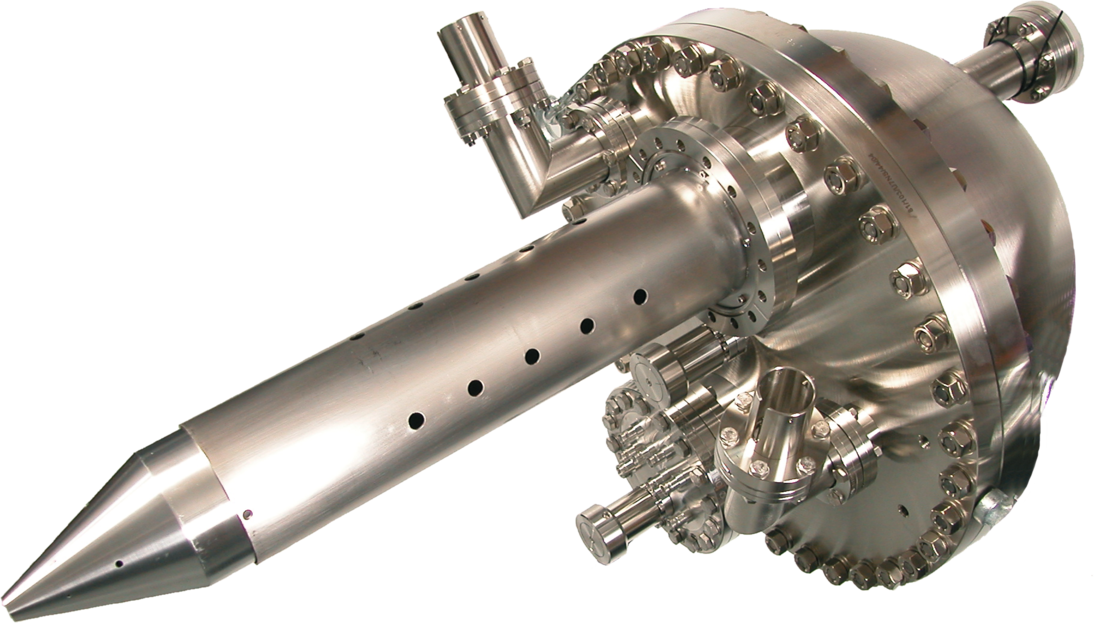
The NanoSAM EA is a hemispherical energy analyser that has been optimised for the best performance in Scanning Auger Microscopy (SAM). Its large acceptance angle of about ± 10°, high transmission, and multi-channel detector (7 channeltrons) are the ingredients to achieve an excellent sensitivity and thus reduced measurement time.
The slim lens geometry makes it possible to bring the analyser lens close to the SEM column and leaves sufficient of the precious space around the SEM column for other detectors and excitation sources, while it also allows tilting of the sample within a large range to mitigate topography shadowing effects.
A lens-integrated octopole deflector is used to compensate the magnetic stray field of the SEM column. An interpolation algorithm choses the correct octopole potentials depending on the beam energy, yet leaving the possibility of manual optimisation for delicate measurements at low kinetic energies.
A set of variable apertures and magnification modes allows the user to chose the best balance between energy resolution and transmission to meet the needs of his application best. Two modes are available for the relation between kinetic and pass energy: the constant retard ration (CRR) mode, which is typically used for Auger electron spectroscopy and microscopy, and the constant analyser energy (CAE) mode, which is employed for XPS if an X-ray source is available on the system.
The NanoSAM EA is controlled through Scienta Omicron’s MATRIX software for electron spectroscopy, both for Auger and X-ray photoelectron spectroscopy. The MATRIX software is integrated with Zeiss’ SmartSEM software and includes features such as drift compensation for long-term measurements and a periodic table of the elements with typical electron peak energies. Data can be exported into standard formats such as VAMAS or ASCII for subsequent data processing with analysis software, e.g. Casa XPS. A software module for automated execution of batch jobs such as sputter depth profiling using Auger electron spectroscopy for the elemental composition analysis is also included.
Specifications
Guaranteed specification: < 1x10 -10 mbar,
acceptance criterion: < 3x10 -10 mbar
10 mm x 10 mm x 10 mm, ± 60°
Limitations by scientific components may apply.
Guaranteed specification: < 40 K
< 0.4 nA beam current: < 6.5 nm
1 nA beam current: < 12 nm
< 0.4 nA beam current: < 5 nm
1 nA beam current: < 7.5 nm
< 0.4 nA beam current: < 3 nm
1 nA beam current: < 4 nm
28 nA beam current: < 18 nm
50 nA beam current: < 12 nm
1 nA beam current: < 13 nm
1 nA beam currnet: < 3 nm
0.1 - 30 keV
