Applications
Our systems and solutions are used by researchers across the globe to grow and analyze new materials used in a wide variety of applications. Below are descriptions of some of the more common applications for those interested in some more information.
Bandstructure Mapping
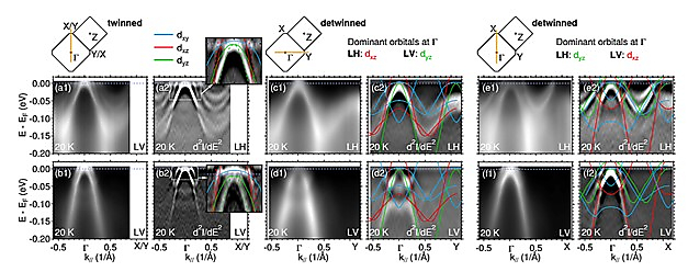
The valence and conduction band electron states in solids determine the properties of the materials. Depending on the bandstructure a material can be a conductor or an insulator, have a specific colour, shows magnetics properties etc. The quantum mechanical wavefunctions of the electrons in a periodic potential displays an energy dependence (dispersion) depending of the degree of overlap of the atomic constituents and the symmetry of the atomic arrangement in the solid.
Graphene
Graphene has attracted large attention after single layers of graphite were isolated for the first time by Andrei Geim (Nobelprize 2010). Although graphite is a known two-dimensional layered material, the electronic structure is close to a semi metal with the valence and conduction bands touching at the Fermi level leading to a very small density of states at the Fermi level. However for a single layer of graphite, graphene, two bands with unequal symmetry cross at the Fermi level giving rise to Dirac cones (linear dispersion of electron states near the Fermi level). This property predicts an extreme high mobility of the charge carriers and is therefore of huge interest in the semiconductor technology.
Interfaces and Buried Thin Films
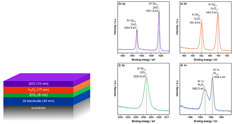
The chemical analysis of buried interfaces and thin films is mainly done through destructive methods like depth profiling XPS or SIMS. However the removal of material has generally major impact of the chemical state of the material and valuable chemical information is lost. With hard x-ray photoelectron spectroscopy the meanfree path of the primary photoelectrons is much larger and therewith the probing depth. HAXPES can probe buried interfaces and thin films to a depth of appr 50 nm without material removal or influencing the underlying chemistry.
Luttinger Liquids
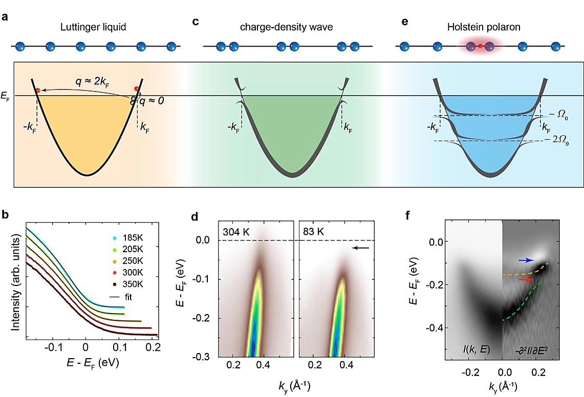
Luttinger liquids are one dimensional fermion (electron) systems. The Luttinger theory predicts a zero conductance at zero temperature for one dimensional metallic system and a power law behaviour just above T=0. Although most of the theory has it signatures at ultra-low temperature, the model is very useful in the description of polarons, plasmons and charge density waves.
Majorana Fermions
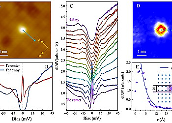
Majorana fermions are a class of quasi particles with the exceptional property to be its own antiparticle. The Majorana fermions can be found in superconductors materials in the superconductor energy gap at zero energy. Conductivity STM measurements of superconducting materials in the gap can demonstrate a peak at zero energy which is a sign of the Majorana fermion or Majorana zero mode.
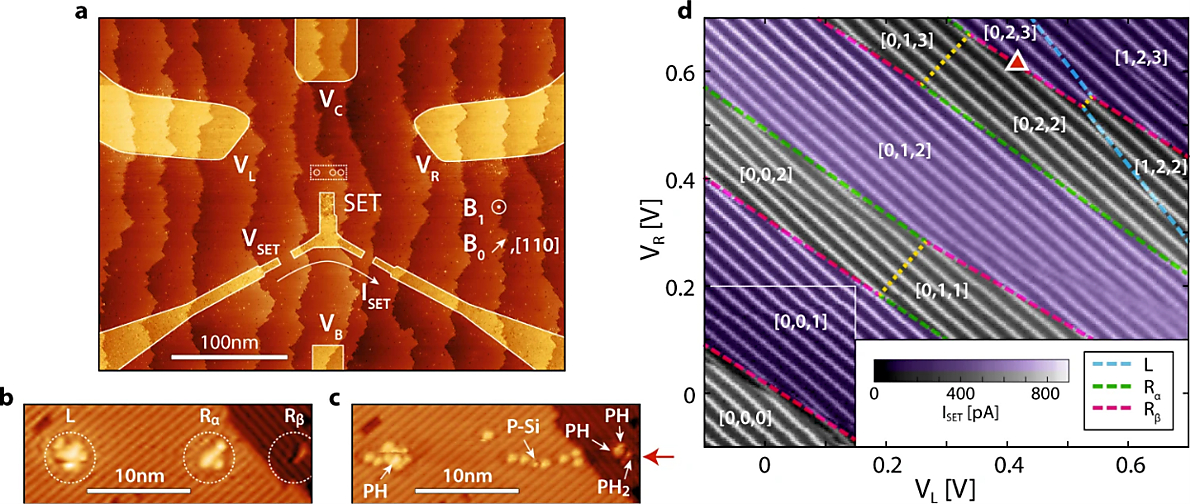
Molecular Electronics
Since the first silicon transistor, the manufacture of transistors in electronics developed rapidly in size (smaller) and density (higher), following Moore’s law: ‘the number of transistors in a dense integrated circuits doubles every two years. The miniaturization of electronics continued following this development until the new millennium. Higher transistor densities and smaller transistor sizes have their ultimate limit at the atomic level. Feynman indicated in 1959 already that ‘there is plenty of room at the bottom’. Fabricating electronic devices based on atoms and molecules is referred to as molecular electronics.
Molecular Orbital Imaging
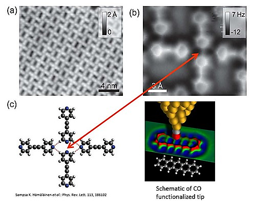
The introduction a quartz tuning fork sensor with a metallic tip on one prong has provided STM with an ultrasensitive sensor that can be used for both scanning tunneling measurements as well as scanning atomic force measurements. Moreover, when multiple channels are registered at the same time (tunneling current, frequency shift and phase shift), the most delicate electronic features can be made visible. The ultimate of such a feature is an individual molecular orbital at specific energies.
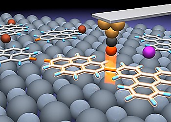
On Surface Synthesis
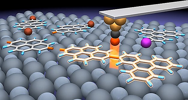
Fabricating nanostructures via on surface synthesis with molecules is interesting for the research in exotic properties of small nanostructures and the development of molecular electronics. In surface synthesis molecular building blocks are connected together by the use of a scanning probe tip or by self-assembly chemical reactions with selective precursors. The STM tip can make and break chemical bonds by applying selective pulse at the right moment and right place.
Picosecond Time Resolved XPS
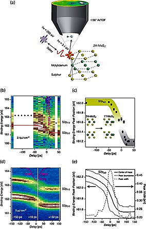
In two photon XPS a laser pulse is synchronized with a pulsed x-ray source like in a single bunch synchrotron mode. The laser pulse can excite the material and change the electronic structure in a very short time domain. The correlated x-ray pulse is than used to excite a core electron in order to probe the modified electronic structure. Changing the delay time of the pulses yield useful information of the electronic mechanisms in the original and modified electronic structure.
Quantum Bits and Quantum Dots
In modern computing the smallest piece of information is the bit. A bit can have two values: 0 or 1. In quantum computing the smallest piece of information is the quantum bit. Similar to the traditional bit it can have the value of 0 or 1, but additionally to the traditional 0 and 1 values a qubit can be in a superposition of both 0 and 1 states. The power of the superpositions in qubits becomes clear when large arrays of high fidelity entangled qubits can be set to specific values with one operation. The power of supercomputing is expected to be orders of magnitude stronger than the current traditional computers. Encryption by quantum computers is likely to be impossible to decrypt by traditional computers and vice versa. Encrypted bitcoins and other current encryptions are decrypted with ease by quantum computers.
Spin Resolved Momentum Microscopy
Spin and angle resolved photoelectron spectroscopy has become very important with the increased attention for topological insulators. In this class of materials the electronic structure of the surface is significantly different than from the bulk. An insulating material can have a conducting surface. Topological insulators with bands crossing the Fermi level at the surface can have spin locked states which yield in a spin polarized charge transport at the surface. The surface properties are highly sensitive for magnetic fields.
STM-Induced Fluorescence
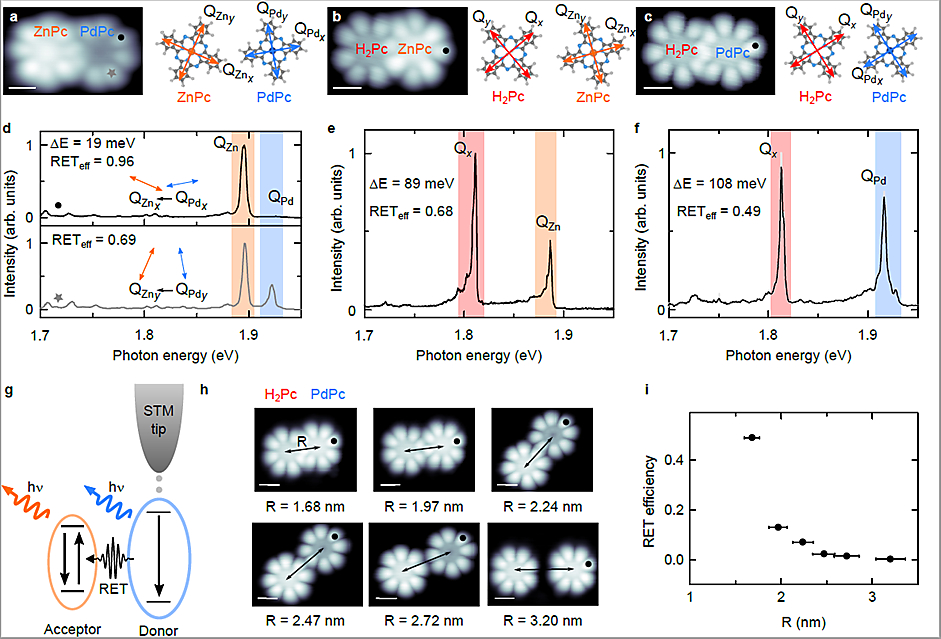
In STM fluorescence the light is collected and analyzed when an electron is injected into an empty state or a hole is created in an occupied state of a molecule or solid. Combining microscopy and spectroscopy molecular electron states can be mapped and individually excited by selective electron injection. In optically active molecules the optical excitation can be addressed directly and optically analysed.
Topological Insulators
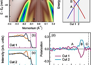
Topological Insulators are a class of materials where the electronic structure and symmetry of the surface is significantly different than from the bulk. An insulating material can have a conducting surface, but for topological insulators the crossing of two bands with different symmetry can lead to sharp Dirac cones near the Fermi level. Conductivity accommodated in these ‘Dirac states’ is expected to be extremely high due to the extreme (infinite) electron mobility.
Twisted Graphene
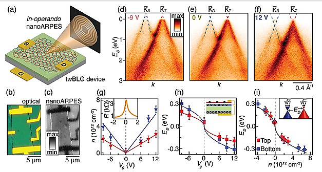
Graphene has attracted large attention after single layers of graphite were isolated for the first time by Andrei Geim (Nobelprize 2010). Although graphite is a known two-dimensional layered material, the electronic structure is close to a semi metal with the valence and conduction bands touching at the Fermi level leading to a very small density of states at the Fermi level. However for a single layer of graphite, graphene, two bands with unequal symmetry cross at the Fermi level giving rise to Dirac cones (linear dispersion of electron states near the Fermi level). This property predicts an extreme high mobility of the charge carriers and is therefore of huge interest in the semiconductor technology. In twisted bilayer graphene a superimposed super structure is created depending on the twist angle. With the tuning of the twist angle the superimposed periodicity can be controlled and there with properties the influence the electronic behavior from insulators to superconductors.