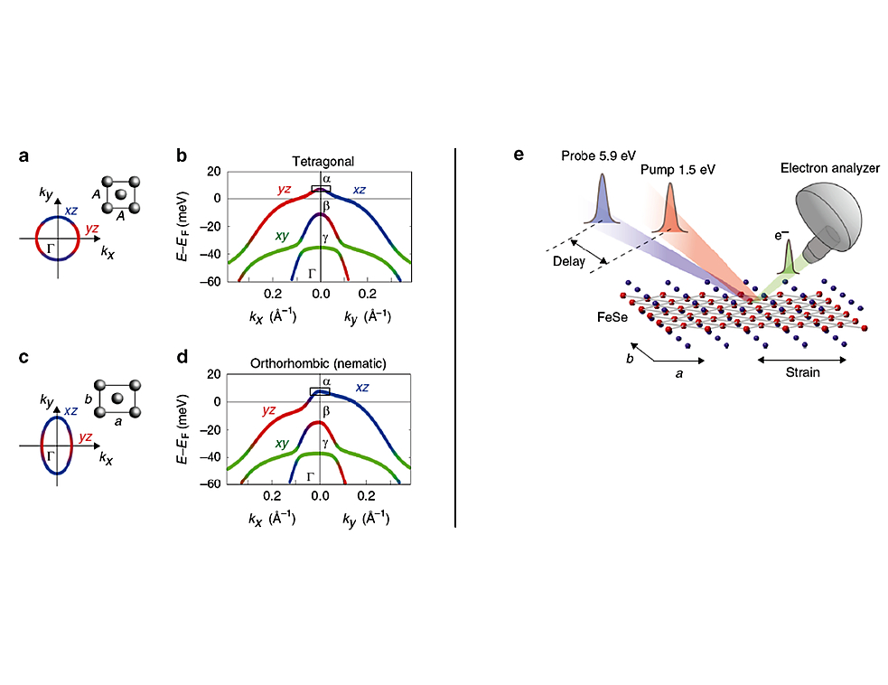
Electronic structure of FeSe and experimental setup for TARPES. (a) Schematic Fe lattice and Fermi surface around the Γ point in the tetragonal phase. x and y are coordinates along the crystal axes of the orthorhombic
setting a and b (a > b), respectively. (b) Band dispersions and orbital characters in the tetragonal phase obtained by a band calculation including the spin–orbit coupling17. α, β, and γ denote the outer, middle, and inner
hole band, respectively. (c, d), The same as a and b but for the orthorhombic phase. For reproducing the ARPES results (Supplementary Note 1), the spin–orbit coupling and orbital polarization were included in the band
calculations in (d) (ref. 17). € Schematic experimental geometry of TARPES on detwinned bulk FeSe. Taken from [1] (CC BY 4.0) [2]
[1] T. Shimojima et al., Nature Comm 10 (2019) 1946
[2] http://creativecommons.org/licenses/by/4.0/
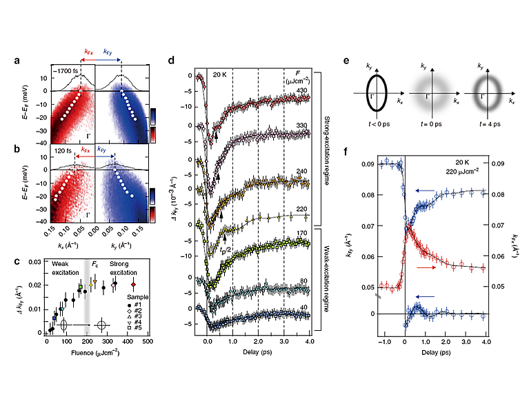
Ultrafast transformation of the nematic Fermi surface. (a) E–k images in a logarithmic color scale obtained by p-polarized probe laser of hν = 5.9 eV along kx (left panel) and ky (right panel) axes at 20 K, before photo-excitation of F = 220 μJ cm−2 (t = −1700 fs). Black curves represent the momentum-distribution curves (MDCs) at the EF and the broken black lines indicate their peak positions. White markers show the band dispersions obtained from the MDC peaks. (b) The same as a but after photo-excitation (t =120 fs). (c) F dependence of the kF shift along ky (ΔkFy) at t = 120 fs. Fc represents the F where the C4 symmetric Fermi surface is attained after the photo-excitation. (d) F dependence of ΔkFy(t). The data set was obtained at 20 K from five single crystals as indicated by the different markers in (c). (e) Schematics of the Fermi surface around the Γ point for t < 0 ps, t = 0 ps, and t = 4 ps deduced from the transient kFx and kFy, and the width of the MDCs at the EF. (f) Transient kFy (blue open circles) and kFx (red open circles) as a function of delay time with the fitting functions (black curves). Damped oscillation in kFywas extracted by subtracting the exponential decay components, as shown in the bottom. Taken from [1] (CC BY 4.0) [2]
[1] T. Shimojima et al., Nature Comm 10 (2019) 1946
[2] http://creativecommons.org/licenses/by/4.0/
In this Nature paper, T. Shimojima (RIKEN CEMS) et al. use time-resolved ARPES to visualize the ultrafast dynamics of electronic nematicity in FeSe. By probing detwinned crystals with different linear polarizations of their pulsed laser system (250 fs time resolution), they can selectively observe xz and yz orbital electrons. The time-resolved ARPES measurements were acquired with Scienta Omicron’s R4000 electron analyzer at the University of Tokyo (ISSP).
The electronic nematic phase is an unconventional state of matter that spontaneously breaks the rotational symmetry of electrons. In iron-pnictides/chalcogenides and cuprates, the nematic ordering and fluctuations have been suggested to have as-yet-unconfirmed roles in superconductivity. However, most studies have been conducted in thermal equilibrium, where the dynamical property and excitation can be masked by the coupling with the lattice.
Here we use femtosecond optical pulse to perturb the electronic nematic order in FeSe. Through time-, energy-, momentum- and orbital-resolved photo-emission spectroscopy, we detect the ultrafast dynamics of electronic nematicity. In the strong-excitation regime, through the observation of Fermi surface anisotropy, we find a quick disappearance of the nematicity followed by a heavily-damped oscillation. This short-life nematicity oscillation is seemingly related to the imbalance of Fe 3dxz and dyz orbitals. These phenomena show critical behavior as a function of pump fluence. Our real-time observations reveal the nature of the electronic nematic excitation instantly decoupled from the underlying lattice.
Author(s):
T. Shimojima1,2, Y. Suzuki2, A. Nakamura1,2, N. Mitsuishi2, S. Kasahara3, T. Shibauchi 4, Y. Matsuda3, Y. Ishida5, S. Shin5 & K. Ishizaka1,2
Institute(s):
1) RIKEN Center for Emergent Matter Science (CEMS), Wako 351-0198, Japan.
2) Quantum-Phase Electronics Center (QPEC) and Department of Applied Physics, The University of Tokyo, Tokyo 113-8656, Japan.
3) Department of Physics, Kyoto University, Kyoto 606-8502, Japan.
4) Department of Advanced Materials Science, The University of Tokyo, Kashiwa 277-8561, Japan.
5) Institute for Solid State Physics (ISSP), The University of Tokyo, Kashiwa 277-8581, Japan.
This website uses cookies
We use cookies to personalise content and ads, to provide social media features and to analyse our traffic. We also share information about your use of our site with our social media, advertising and analytics partners who may combine it with other information that you’ve provided to them or that they’ve collected from your use of their services