Realization of a two-dimensional Weyl semimetal and topological Fermi strings
Result of the Month
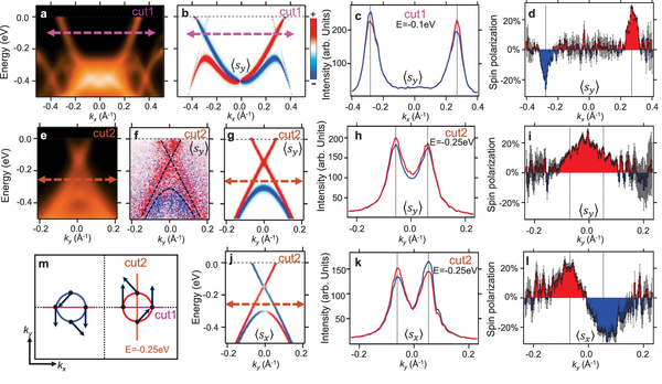
a ARPES spectrum along “cut1” along a high symmetry line. b Calculated band structure along “cut1” with the inclusion of photoemission matrix elements. The bands are colored according to the calculated expectation value 〈sy〉 of each state. c Spin-resolved momentum distribution curves (MDC) taken at E = −0.1 eV along the line marked by the pink dashed arrows in (a) and (b). The blue and red curves are the photoelectron intensity recorded in the “spin-down” and “spin-up” channels of the spin detector, respectively. d The spin polarization extracted from the MDCs in (c). The shaded area indicates net spin polarization of 〈sy〉. e ARPES spectrum along “cut2” marked in Fig. 2a. f 2D spin-resolved ARPES map of 〈sy〉 taken along “cut2''. The blue and red dots represent the photoelectron signals recorded in the “spin-down” and “spin-up” channels of the spin detector, respectively. g Calculated electron band structure along “cut2'', which is colored according to the expectation value 〈sy〉 of each state. h Spin-resolved MDCs of 〈sy〉 taken at E = −0.25 eV along the line marked by the green dashed arrows in (e) and (g). i Spin polarization of 〈sy〉 extracted from the MDCs in (h). j–l Same as g–i, but for the spin component 〈sx〉. m In-plane spin texture of iso-energy contours at E = −0.25 eV. The red and blue circles schematically depict the iso-energy contours of two valleys at E = −0.25 eV. The black arrows indicate the in-plane spin orientation of the Weyl fermion states.
The acquisition time for spin-resolved measurements in figure (c) and (f) was one and several hours respectively.
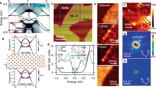
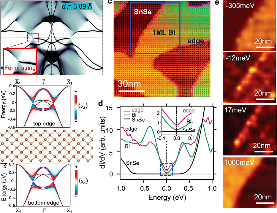
(a) The edge bands and projected bulk bands of a semi-infinite bismuthene film on SnSe with an open boundary in the (010) direction. The bands are weighted with the charge density near the edge. d0 = 3.89 Å is the relaxed interlayer spacing between bismuthene and SnSe substrate. b) The connection of Fermi string edge bands to bulk Weyl nodes. The band structure was calculated by using a tight-binding model in which sz is conserved. (c) STM topography of bismuthene on SnSe. d Differential conductivity dI/dV spectra with the bias voltage aligned with the energy of Weyl nodes. The green curve is the averaged spectrum taken at the green grid inside the bismuthene patches shown in (d). The black curve is the averaged spectrum from the black grid on the surface of SnSe. The magenta curve is the averaged spectrum from the magenta points at the edges of the bismuthene patches. The inset shows the zoom-in dI/dV curves around the energy of Weyl nodes. (e) dI/dV map over the area marked by the blue box in c at bias voltage V= −305, −12, 17, and 1000 meV. f High-resolution dI/dV map at bias voltage V = +10 meV. g The corresponding Fourier transform of the dI/dV map in f, showing the quasiparticle interference (QPI) pattern. h The calculated quasiparticle interference pattern with spin-dependent scattering probability is considered.
The result of quasiparticle interference pattern obtained with STM (g) agrees well with theoretical calculation (h) and the ARPES results (shown in figure 2a in the original publication).