ACCESS-HAXPES
XPS and HAXPES as-a-Service for Advanced Surface Analysis
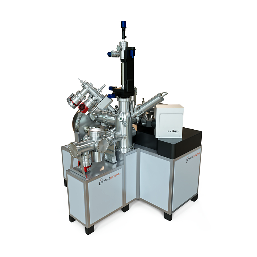
Non-destructive, bulk-sensitive analysis for cutting-edge research and development
Gain access to the unparalleled power of high energy XPS (HAXPES) without the need for capital investment. We deliver cutting-edge material analysis tailored to your needs, offering precision, speed, and flexibility.
We specialize in delivering XPS and advanced Deep HAXPES measurements to academic and industrial laboratories. Our service integrates state-of-the-art technology, innovative methodologies, and expert support to help you uncover new insights into material interfaces and properties.
Unique information by Deep HAXPES:
- Non-destructive & bulk-sensitive depth profiling
- Access to buried interfaces
(up to 50 nm below the material surface) - Access to sub-surface chemical and electronic material properties
- Operando measurement possibilities
Applications, features and benefits
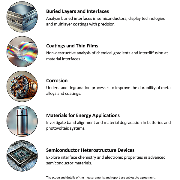
Core Features
- Standard and high energy XPS (Deep HAXPES)
- Non-destructive and bulk-sensitive analysis
- Elemental characterization by XPS and Deep HAXPES
- Chemical characterization of the elemental composition up to 50 nm below the sample surface
Benefits
- Quick turnaround time for results
- Comprehensive analysis reports with metadata
- Flexible measurement time agreements
Add-Ons
- Advanced analysis services upon request
Application notes
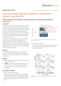
Accurate Oxygen Vacancy Profiling in Ferroelectric Hafnia Using HAXPES
Keywords: Ferroelectric devices, Non-volatile memory, Defect engineering
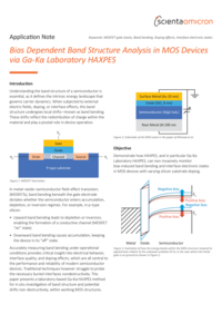
Bias Dependent Band Structure Analysis in MOS Devices via Ga-Kα Laboratory HAXPES
Keywords: MOSFET gate stacks, Band bending, Doping effects, Interface electronic states
Surface Characterization of Mesoporous NiOx Using Ga Kα HAXPES
Keywords: Energy storage, Catalysis, and Sensing
Revealing Hot-Electron Dynamics in Plasmonic Nanohybrids Using XPS and HAXPES
Keywords: Photocatalysis, Plasmonics, Energy conversion, Advanced spectroscopy
Revealing subsurface chemistry and defect dynamics with HAXPES
Keywords: Thin film, Buried interface characterization, Oxide electronics, Ferroelectric
Interface Chemistry and Thermal Boundary Resistance in Ru/TaN/SiO₂ Interconnects Revealed Using Ga-Kα Laboratory HAXPES
Keywords: Semiconductor interconnects, Thermal management, Buried interfaces engineering for VLSI, Metrology
Get in touch with us at info@scientaomicron.com