LT NANOPROBE Lab
Transport Measurements at the Atomic Scale
SPM LT SPM STM STS LT STM HDL Manipulation Nanolithography 4P-SPM AFM nc-AFM QPlus AFM
- Four independent atomic resolution SPMs
- Extremely low thermal drift at T < 5 K
- SEM imaging for rapid tip navigation
- STM spectroscopy and atom manipulation
- QPlus® nc-AFM
The Low Temperature NANOPROBE defines a new class of analytical instruments that merges SEM-navigated local transport measurements with atomic scale precision, high performance STM imaging, spectroscopy, and manipulation at LHe temperatures.
“QPlus® is a registered trademark of Professor Franz J. Giessibl, Regensburg, Germany”
More Information
Cooling Down to T < 5 K

The use of a high-resolution SEM column for tip navigation from above implies an unconventional cryostat concept. A specifically designed bath cryostat with LN2 and LHe reservoirs allows for a measurement time of > 45 hours at T < 5 K and cools the whole microscope stage from below.
Thermal shielding

LN2 and LHe double shields minimise the thermal impact on the stage. Doors to exchange tips or samples are operated by wobble stick. As the UHV Gemini column uses an in-lens secondary electron detector, the thermal impact during SEM imaging is minimised and the microscope stage main- tains the minimal temperature of T < 5 K during SEM operation.
Four SPMs

The microscope stage carries four individual SPM modules with independent and guided 3D coarse positioning of XYZ = 5 x 5 x 3 mm. The sample can be independently positioned by XY = 4 x 4 mm. Our patented piezo-electric inertia drives provide highly reliable and efficient navigation with step sizes from a few tens of nm´s up to several hundred nm. Fine positioning and atomic resolution STM imaging is achieved by shared stack scanners with a range of 1.5 µm x 1.5 µm at 5 K. For ultimate STM performance the microscope stage employs an effective eddy current-damped spring suspension.
Sample & tip exchange
A fast and secure tip and sample exchange is crucial for ease of use and high throughput. Samples and spring loaded tip carriers can easily be exchanged by wobble stick.
Thermal shielding
An efficient thermal shield compartment allows for temperatures well below 5 K, extremely low thermal drift and thermal equilibrium of sample and probes. In addition, high resolution SEM navigation requires a small SEM working distance and thus makes a dedicated STM concept indispensable. A sophisticated shared stack scanner allows for a very compact and flat design, while ensuring highly linear, orthogonal and stable STM scanning characteristics.
Smart sample and tip transfer
The possibilities for smart transfer of tips and samples throughout the complete UHV chamber and into the LT NANOPROBE stage are fundamental for comfortable routines and processes.
Fast Entry Locks
The LT NANOPROBE offers two different fast entry locks (FEL), located opposite to each other on both sides of the system. This positioning allows for easy provision of tips and samples. Two wobble sticks - both right angled to the transfer rods of the FEL - are taking over the 'inner tasks' like adjustment, handling, positioning or 'parking' of tips and samples within the 28-position-carousel. Various lock valves assure for short pump-down times as well as stable vacuum conditions.
Pumping system
The pumping is realized via efficient turbo- and ion-pumps. The manipulator in the preparation chamber allows for tip and sample preparation, sputtering and depositioning.
Two-probe STM experiments at the atomic level
The unprecedented stability and drift performance of the LT NANOPROBE opens the route towards multi-probe transport measurements of planar atomic or molecular nano-scale systems.
So far the stability of single atom contacts and probe navigation with real atomic precision has only been accessible by single probe SPM experiments. Parallel STM imaging of probes is crucial to control the individual points of contact and to identify the minimal distance between probes by inter-probe tunnelling.
Electronic structure of Ge(001)-c(4 × 2)
-c(4 x 2) surface and two probe experimental setup | © Marek Kolmer et al.")
Marek Kolmer et al., Nature Comm 10, 1573 (2019) DOI: s41467-019-09315-6
Fig. 1 Electronic structure of Ge(001)-c(4 × 2) surface and two-probe experimental setup. a Side and top views of the used unit cell, twice the size of the primitive cell, and the corresponding Brillouin zone (see Supplementary Fig. 16 for details). Yellow and orange colored Ge atoms highlight the buckled wire. b Calculated band structure of a 12-layer Ge(001)-c(4 × 2) slab. The red box highlights the dispersive surface-state bands #1–4. Positions of the conduction band edges CBE (bottom of bands #1 and #2), CBE+1 (bottom of bands #3 and #4) and CBE+2 (top of bands #1–4) correspond to the resonances in the projected density of states (see Supplementary Fig. 17 for details). The bulk Ge band structure is shown in shaded gray (details of the band alignment of slab and bulk are presented in Supplementary Note 10). Notice that the CBE+2 position overlaps with the onset of the bulk conduction band. c Model presentation of the experimental setup. Both tips are kept in the tunneling regime above a grounded sample. Bias voltage is applied to tip1, whereas tip2 is virtually grounded through its preamplifier. Corresponding currents are registered on both tips. d Two-probe measurement scheme for the transconductance dI2/dV1 signal, which probes the energy positions of ballistic transport channels mediated by the surface states. The experimental design resembles the ballistic-electron emission microscopy concept64–66 with tip2 acting as a collector. The schematic surface density of states (blue) shows the three discussed resonances, associated with the edges of the two quasi-1D surface bands (whose density of states are represented in green and orange). Notice that the Fermi energy of Ge(001) is known to be pinned at the top of the Ge bulk valence band43,44,62,63. Thus, in our scheme the chemical potentials of tip2 and the surface are aligned.
Molecule manipulation

Long range manipulation using tip 2 while scanning the surface in parallel with tip 4. The 4-Acetylbiphenyl molecule-automobile (ABP) [1] was driven by inelastic tunneling effect, with the manipulation parameters determined first by TU Dresden in 2013 [1,2]. Image sequence taken on a Au(111) surface with the 0.25 Ang surface corrugation clearly visible in the background and a 1.8 Ang corrugation for the moving ABP molecule. Sequence of 50 minutes (pulses and images) for a first long run of about 4 nm. No mechanical manipulation. Data obtained during the TU Dresden team trainingsession for the nanocar race at the PicoLab in Toulouse.
Video
On the LT NANOPROBE, it was possible for the first time to manipulate a single molecule on the long range using the tip 2 of this instrument while scanning the surface in parallel with tip 4. This 4-Acetylbiphenyl molecule-automobile (ABP) [1] was driven by inelastic tunneling effect, with the manipulation parameters determined first by TU Dresden in 2013 [1,2]. Image sequence taken on a Au(111) surface with the 0.25 Ang surface corrugation clearly visible in the background and a 1.8 Ang corrugation for the moving ABP molecule. Sequence of 50 minutes (pulses and images) for a first long run of about 4 nm. No mechanical manipulation. Data obtained during the TU Dresden team training session for the nanocar race at the PicoLab in Toulouse.
Simultaneous atomic resolution on Au(111) with all for SPMs
 73.")
Atomic resolution constant current STM images of Au(111)-(1×1) surface recorded with the scanners PS1, PS2, PS3 and PS4 with in each case an optimized 45° oriented tip. The central SEM image is illustrating the position of each tip during the scanning. The size of all the STM images is 3 nm × 1.5 nm recorded at 200 pA for a 500 mV bias voltage. The difference in corrugation between each image indicates the different tip apex used per scanner. Those images can be recorded independently and in parallel.
Data courtesy by Ch. Joachim, Eur. Phys. J. Appl. Phys. (2016) 73.
Low thermal drift

The thermal stability and resulting thermal drift of the whole microscope stage - four probe modules relative to the sample - is crucial for long-term measurements on nm-sized structures. It essentially defines the time window for sequential positioning of the four probes and the measurement time, during which probes can be held in electrical contact at atomic scale dimensions. The excellent drift performance in the few A /h regime also enables single or multi-tip tunnelling spectroscopy experiments.
STM atom manipulation on Au(111) at T<5K

The LT NANOPROBE stability virtually matches state-of-the art performance of well-established single tip low temperature STMs and therefore enables extended experiments such as atom and molecule manipulation and tunnelling spectroscopy.
Constant current STM images of a 20 nm × 16 nm Au(111) surface where many single Au ad-atom have been manipulated in a constant current pushing mode to construct a letter C with 6 Au ad-atoms. A total of 11 Au ad-atoms have been manipulated 6 for the C and 5 to clean the surface around the C.
Tip re-positioning accuracy

Tip re-positioning accuracy is important as an individual tip needs to be retracted from tunnelinng distance during the other tips are approached and positioned using their 3D coarse motors. When the positioning process of all for tips is finished, tips are approached back into tunnelling conditions with atomic precision.
QPlus AFM on NaCl (001) at T < 4.5 K

QPlus non-contact AFM imaging of NaCL(001) at T < 4.5 K simultaneously acquired with 2 scanners (plane substract only).
Left: vSCAN = 1.6 nm/s, VTip = 0V, DfSET = -5.06Hz, AOSC = 0.55nm, fRES = 21.3 kHz, Q ≈ 111k
Right: vSCAN = 1.11 nm/s, VTip = 0V, DfSET = -5.06Hz, AOSC = 0.55nm, fRES =22.6 kHz, Q ≈ 48k
Results
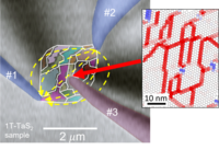
Manipulation of Fractionalized Charge in the Metastable Topologically Entangled State of a Doped Wigner Crystal
Metastability of many-body quantum states is rare and still poorly understood. An exceptional example is the low-temperature metallic state of the layered dichalcogenide 1T-TaS2 in which electronic order is frozen after external excitation....
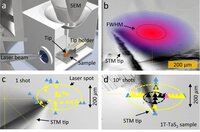
A Time-Domain Phase Diagram of Metastable States in a Charge Ordered Quantum Material
Metastable self-organized electronic states in quantum materials are of fundamental importance, displaying emergent dynamical properties that may be used in new generations of sensors and memory devices. Such states are typically...
Reference Systems


 | © Penn State University")
Downloads
LT NANOPROBE: Atomically Precise Electrical Probing
The Low Temperature Nanoprobe defines a new class of analytical instrumentation that merges SEM-navigated local transport measurements with atomic scale precision, high performance STM imaging, spectroscopy, and manipulation at LHe temperatures. The key features include 1) transport measurements with atomic scale precision; 2) independent atomic resolution SPMs for probe approach and imaging; 3) extreme low thermal drift at T < 5 K; 3) simultaneous SEM imaging at low temperature for rapid tip navigation; 4) STM spectroscopy and atom manipulation; and 5) QPlus® nc-AFM.

MATRIX 4: The SPM Controller Evolution
The MATRIX 4 Control System builds on 30 years of experience in SPM technology and unlocks the full capacity of our leading-edge Scanning Probe Microscopes. The key features include intuitive and flexible experiment control; best-in-class noise floor; full 64-bit software; and modular upgrade paths.
Zyvex CHC Controller
Scienta Omicron and Zyvex Labs announce a new leap forward in STM design; real- time position correction. The ZyVector STM control system from Zyvex Labs uses live position correction to enable atomic-precision STM lithography. Now the same live position correction technology is brought to the Matrix STM control system for microscopy and spectroscopy users, enabling fast settling times after large movements in x, y and z, and precise motion across the surface, landing and remaining at the desired location.


