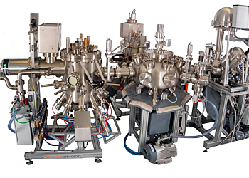
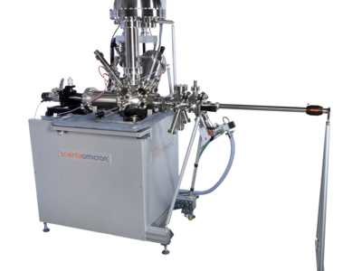
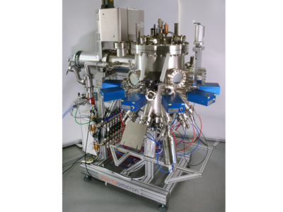
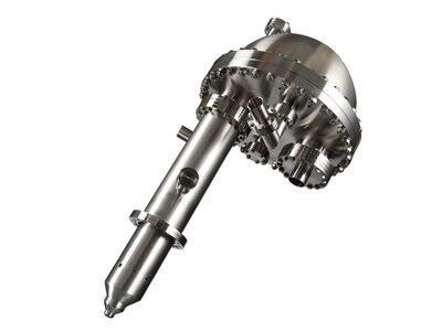
The Group´s approach utilises advanced molecular beam epitaxy techniques, selective area atomic layer deposition, and highly developed materials characterisation to fundamentally understand the nucleation and growth process, material nanostructure, chemical bonding, and experimentally determined band structure. They then correlate those findings with advanced electrical transport and magnetic measurements from devices that they fabricate to take full advantage of the novel properties of the materials and heterostructures that are created. Their current research interests include semiconductor defects for quantum communication, topologically protected transport in semiconductors and metals, magnetic properties in 2D materials, and back-end-of-line materials and device integration.
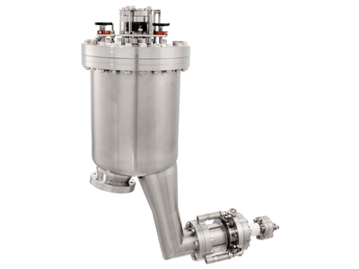
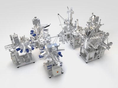
- EVO-50 MBE for Oxides - 2" wafer - O plasma source
- EVO-50 MBE for TMDC - 2" wafer - N plasma source
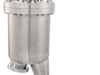
- ALD Lab for small samples
- XPS Lab - 2" wafer compatible – with Argus CU and monochromated X-ray source
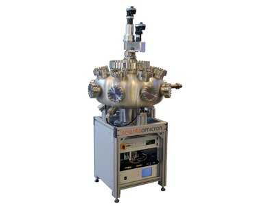
- Radial Distribution Chamber
