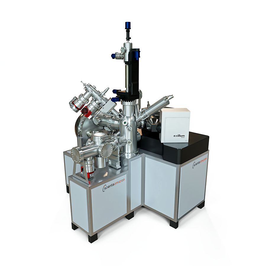
DeepCore-X
Investigate surface to interface, without sputtering, without compromise
- Synchrotron-like performance in your own lab enabled by the high-flux Ga Kα (9.25 keV) F-series MetalJet source.
- Surface precision and bulk access in one instrument with dual excitation from Al Kα (1.5 keV) for surface sensitive XPS and Ga Kα for HAXPES with up to ~50 nm information depth.
- More data in less time with high accuracy using the EW4000 analyser for highest transmission and efficient depth profiling.
- Minimal hands-on time and reduced errors through automation, guided sample introduction, camera navigation, and easy access sample library.
Designed for advanced surface and bulk materials research, DeepCore-X enables high-resolution X-ray Photoelectron Spectroscopy (XPS) and Hard X-ray Photoelectron Spectroscopy (HAXPES) in a single, laboratory-based instrument. With its high-flux Ga Kα MetalJet F-series source (9.25 keV) and the synchrotron-proven EW4000 analyser, DeepCore-X delivers synchrotron-like performance while maintaining ease of use in a compact system. Automation of sample handling, smart workflows, and camera-assisted navigation make DeepCore-X a highly productive and accessible platform for every level of expertise.
Need HAXPES measurements on your samples?
Explore are on-demand analysis service: ACCESS-HAXPES
When combined with Scienta Omicron’s Materials Innovation Platform (MIP), DeepCore-X can be integrated with in-situ deposition and complementary analysis techniques for a complete materials research solution. Designed with sustainability in mind, DeepCore-X features long-lifetime components, modular upgrade paths, and efficient operation that reduces environmental impact while maximizing productivity.
More Information
9.25 KeV Ga Kα source from Excillum
-
Non-destructive Deep HAXPES access to buried interfaces and bulk – enabled by Ga Kα (9.25 keV) hard X-rays.
-
High flux for fast HAXPES – 1000 W continuous operation with ~3.5× intensity boost (F vs D-series) accelerates data collection.
-
Sharp spectra on small features – ~50 μm spot enabling grazing incidence synchrotron beamline geometry.
-
F-series, engineered for uptime – liquid-metal jet with electromagnetic pump (no moving parts), jet shield and exit-window protection for stable and reliable operation.
EW4000 High-Energy Electron Analyser

- More data per run, less stage motion – 60° extreme wide angular acceptance and 200 mm radius, for highest transmission and efficient depth profiling.
- Resolution and flexibility for any task – variable pass energy (20–500 eV), swept and snapshot modes, and software-controlled entrance slits optimize count rate vs. resolution.
- Clean signals and reproducibility – low-noise 2D MCP/digital camera detector and ultra-stable HV electronics deliver consistent, publication-grade, high signal-to-noise XPS and HAXPES spectra.
- Accurate acquisitions with minimal distortion – built-in image-correction software ensures reliable energy and emission-angle imaging, even at wide acceptance, for all combinations of settings.
Flexible sample handling with multiple carrier options

DeepCore-X is designed for easy access to a wide range of samples, supporting both regular research use and advanced experimental needs. It enables maximum throughput, reproducibility, and versatility in both shared environments or dedicated research labs
-
Multiple carrier options allow users to work with everything from small research specimens to large or specialized substrates, ensuring compatibility across disciplines.
-
Quick sample exchange and intuitive handling reduce downtime, making the system efficient for core facilities and multi-user labs.
-
Optimized chamber and manipulator design provide stable positioning and precise alignment, essential for reproducible results.
-
Future-proof flexibility — modular carriers can be adapted or upgraded to meet evolving research requirements.
Integrated control and acquisition software

Our new software unifies instrument control and data acquisition into one seamless environment, ease of use, transparency, and productivity, letting researchers focus on insights instead of setup.
-
Flexible workflows simplify complex tasks like sample introduction, alignment, and measurement setup.
-
Customizable menus and dashboards give users direct control of the system while keeping critical status information visible.
-
Smart automation enables sample queues, unattended runs, and repeatable measurement sequences, boosting throughput and reproducibility.
-
Live visualization provides immediate feedback on spectra and system performance, accelerating decision-making during experiments.
-
Data management tools link measurements to sample metadata, ensuring traceability and easy integration into research workflows.
From HAXPES Lab to DeepCore-X
DeepCore-X is the next generation of our laboratory HAXPES instrument, evolving from the widely installed HAXPES Lab. While the name has changed, the scientific foundation remains the same. All published results, application notes, and reference systems built on HAXPES Lab continue to be directly relevant to DeepCore-X, which extends the platform with higher flux, smarter automation, and enhanced usability.
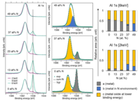
Deep HAXPES 50 nm probing depth
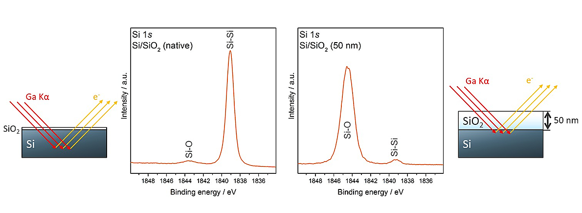
The high-intensity, high-energy Ga Kα X-rays from the MetalJet source generate photoelectrons with very high kinetic energy, offering unparalleled depth sensitivity among laboratory hard X-ray systems. As shown in the figure, the bulk silicon peak is detectable through 50 nm of SiO₂, demonstrating that buried layers and interfaces at device-relevant depths are accessible. Ga Kα, Deep HAXPES allows for the extraction of chemical information from deeper layers of the devices than is possible with Al or Cr-based systems, all within efficient time scales.
Direct observation of band structure variation during device operation

Understanding how buried interfaces respond under electrical bias is critical for evaluating advanced MOS structures and multilayer devices. Traditional surface-sensitive XPS cannot probe through the top electrode and thin film stacks to provide insight of the chemistry in buried layers. Further, lower energies are sensitive to electric fields from sample bias application.

Non-destructive Depth Profiling and Semiconductor Device Interfaces

The high photon energy of the Ga Kα MetalJet source (9.25 keV) allows probing depths of up to 50 nm, making it possible to perform non-destructive depth profiling. By analysing angular intensity distributions and chemical states, layer thicknesses and elemental distributions can be accurately determined, providing valuable insights into device composition and integrity.
Global footprint of Deep HAXPES

DeepCore-X builds on a proven legacy of Scienta Omicron’s Deep HAXPES technology already in use worldwide. From Europe to Asia, North America, and beyond, leading universities, national laboratories, and industrial R&D centers are already using Deep HAXPES
Trusted by leading scientists
– "HAXPES with Ga Kα is transforming characterisation in advanced materials research. We already routinely measure through passivationlayer interfaces and detecting deeply buried layers. The upgraded throughput and sample accessibility of the next generation HAXPES-Lab will enhance this capability significantly.”
Professor Atsushi Ogura

– "Bias-applied operando measurements using Lab HAXPES with Ga x-ray source is a powerful, nondestructive method for evaluating buried interfaces in multilayer films of actual MOS devices. "
Sustainability at the Core

At Scienta Omicron, sustainable product design is our priority, and we believe all research should be carried out with sustainability in mind.
That’s why the Scienta Omicron DeepCore-X has been engineered not only for cutting-edge performance but also for energy efficiency, reduced waste, and long-term reliability.
Specifications
100 mm diameter sample carriers with advanced options for 4” wafers and contacts for bias application
Automatic workflow from entry to measurement
High transmission analyser including angular modes for depth profiling
Monochromated, small spot 9.25 keV (Ga Kα)
Anode: Excillum MetalJet F
Maximum power: 1000 W
Monochromatic 1.49 keV (Al Kα)
Maximum power: 300 W
Yes
Yes
Integrated system control and acquisition software
Gas cluster ion beam source, sample carriers for bias application, 4” wafers, adaptors for flag style samples.
Results
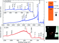
Characterization of Buried Interfaces Using Ga Kα Hard X-Ray Photoelectron Spectroscopy (HAXPES)
The extension of X-ray photoelectron spectroscopy (XPS) to measure layers and interfaces below the uppermost surface requires higher X-ray energies and electron energy analysers capable of measuring higher electron kinetic energies....
Near-Surface Analysis of Magnetron Sputtered AlCrNbYZrNx High Entropy Materials Resolved by HAXPES
Hard X-ray photoelectron spectroscopy (HAXPES) was used to perform a non-destructive depth profile of AlCrNbYZrNx (x = 0 to ∼50 at.%) thin films. The outermost native oxide of the pristine thin films contained the highest coordination...
Electron-donating amine-interlayer induced n-type doping of polymer:nonfullerene blends for efficient narrowband near-infrared photo-detection
Inherently narrowband near-infrared organic photodetectors are highly desired for many applications, including biological imaging and surveillance. However, they suffer from a low photon-to-charge conversion efficiencies and utilize...
The Role of SnF2 Additive on Interface Formation in All Lead-Free FASnI3 Perovskite Solar Cells
Tin-based perovskites are promising alternative absorber materials for lead-free perovskite solar cells but need strategies to avoid fast tin (Sn) oxidation. Generally, this reaction can be slowed down by the addition of tin fluoride...
Reference Systems


Downloads
DeepCore-X Brochure
Designed for advanced surface and bulk materials research, DeepCore-X enables high-resolution X-ray Photoelectron Spectroscopy (XPS) and Hard X-ray Photoelectron Spectroscopy (HAXPES) in a single, laboratory-based instrument. With its high-flux Ga Kα MetalJet F-series source (9.25 keV) and the synchrotron-proven EW4000 analyser, DeepCore-X delivers synchrotron-like performance while maintaining ease of use in a compact system. Automation of sample handling, smart workflows, and camera-assisted navigation make DeepCore-X a highly productive and accessible platform for every level of expertise.
PEAK Brochure
PEAK is designed to control acquisition of photoelectron spectra with Scienta Omicron analysers. With its modern software architecture, PEAK offers improved performance for data acquisition, workflow, and live visualisation of data. The modular design and the modern network-based application programming interface (API) facilitate integration of additional equipment as well as full integration of the analyser in external control systems.
EW4000 Brochure
The EW4000 electron analyser is a state-of-the-art and widely used electron analyser for HAXPES. It is also one of the key parts is Scienta Omicron’s HAXPES Lab. Expanding the parallel angular detection range to 60° in the full range from UPS via XPS to HAXPES gives great possibilities for high transmission measurements as well as novel Standing Wave and XPD experiments.