Valley Interference and Spin Exchange at the Atomic Scale in Silicon
Result of the Month
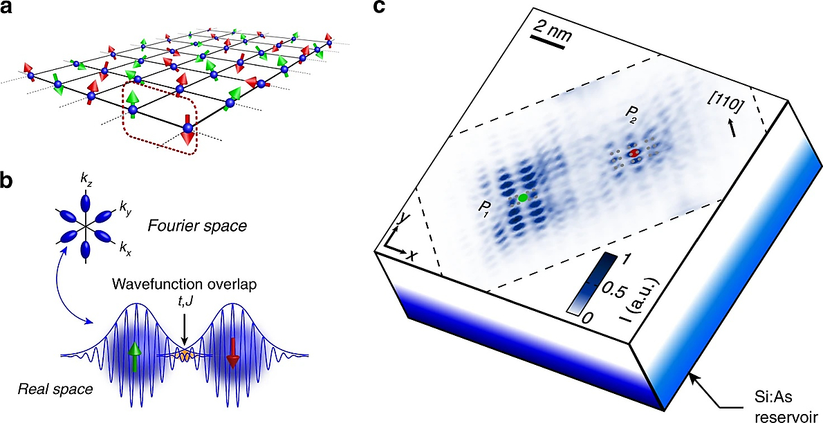
Atomic-scale image of two interacting donors in silicon.
a Schematics of a 2D-array of single electron spins bound to phosphorus atoms in 28Si, where two-qubit operations can occur between nearest neighbours, i.e. red/green spin pairs, using the Heisenberg exchange interaction. b (Top) A donor’s electron wavefunction oscillates at the valley wavevector kμ ~ 0.81k0, with k0 = 2π/a0. Silicon presents a mass anisotropy which results in the donor orbital envelope to be anisotropic as well, as highlighted by their ovoidal shape in Fourier space. (Bottom) Tunnel and exchange interactions result from the overlap between the two donor orbitals, represented by the yellow overlap area, which is sensitive to both envelope decay and valley interference between donors. c Experimental real-space map of the quasi-particle wave function of an exchange-coupled donor pair’s two-electron neutral state. Sequential transport occurs vertically from a highly doped Si:As substrate, which acts as an electron reservoir, to a donor pair found in a low-doped phosphorus δ-layer, and then to the STM tip above (not shown). The red and green dots represent the surface projections of the pinpointed lattice positions of the two donors. The two donors are separated by 6.5a02–√ along [110] (perpendicular to the Si dimers, a0 is the silicon lattice constant), 0.5a02–√/2 (parallel to the Si dimers) along [11¯0], and by 1.25 a0 in depth. The grey dots represent the silicon atom positions of the 2 × 1 reconstructed surface. The black dashed contour indicates the experimentally measured area.
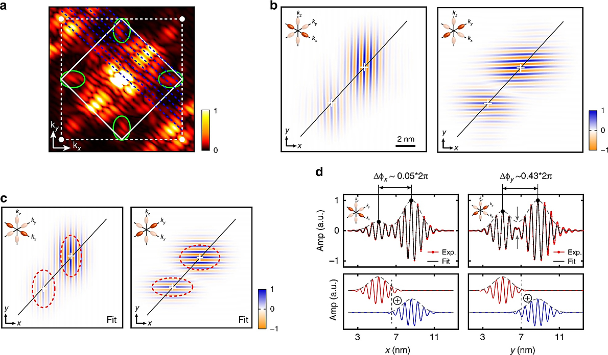
a 2D FFT of the STM image, centred on the first Brillouin zone (solid white lines). The white dots are located at {±k0, ±k0}. The FFT shows a clear valley signal around kμ ~ 0.81k0 evidenced by the green ellipsoids. The FFT also shows diagonal slices (blue dotted lines), cutting through the valley components of the FFT, which evidence the geometric interference between the two donors. b Real-space images of the valley interference, obtained after inverse Fourier transform of the FFT filtered around kx ~ 0.81k0 for the x-valley interference (left) or ky ~ 0.81k0 for the y-valley interference (right). The white crosses indicate the donor positions. The x-valleys look in-phase with the vertical stripes running continuously from one donor to the other. The y-valleys look out-of-phase with a clear discontinuity in the oscillatory valley pattern between the two donors. c 2D fits of the valley images, from which the position of the valley maxima and of the valley frequency, and hence the valley phase differences Δϕx and Δϕy, can be obtained. The red dashed ellipsoids correspond to the donor envelope part of the fits, which highlights their anisotropy. d Line cuts taken through the ion–ion direction of both valley images (red lines) and their fit (black lines), for the x-valleys (left) and the y-valleys (right). The grey dashed lines represent the envelope part of the fits only. The x-valleys are in-phase, which results in the maxima of valley signal to always reach the envelop part. On the contrary, the y-valleys are out-of-phase and the grey arrows in-between the two donors highlight the clear reduction of the valley signal compared to the envelope part as a result of the destructive interference.
Researchers from the ARC Centre for Quantum Computation and Communication Technology (CQC2T) working with Silicon Quantum Computing (SQC) have situated the ‘sweet spot’ for positioning qubits in silicon to scale up atom-based quantum processors. Creating quantum bits, or qubits, by exactly putting phosphorus atoms in silicon is a world-leading approach in the growth of a silicon quantum computer. This method has been pioneered by CQC2T Director Prof. Michelle Simmons. In their research, published in Nature Communications, precision placement has proven to be essential for developing robust interactions—or coupling—between qubits. The team found that there is a special angle, or sweet spot, within a particular plane of the silicon crystal where the interaction between the qubits is most resilient to a valley interference effect. This was located using scanning tunnelling microscope (STM) lithography techniques developed at UNSW, to observe the atomic-scale details of the interactions between the coupled atom qubits, including the valley interference between the atoms and the envelope anisotropy.
Abstract
Tunneling is a fundamental quantum process with no classical equivalent, which can compete with Coulomb interactions to give rise to complex phenomena. Phosphorus dopants in silicon can be placed with atomic precision to address the different regimes arising from this competition. However, they exploit wavefunctions relying on crystal band symmetries, which tunneling interactions are inherently sensitive to. Here we directly image lattice-aperiodic valley interference between coupled atoms in silicon using scanning tunneling microscopy. Our atomistic analysis unveils the role of envelope anisotropy, valley interference and dopant placement on the Heisenberg spin exchange interaction. We find that the exchange can become immune to valley interference by engineering in-plane dopant placement along specific crystallographic directions. A vacuum-like behaviour is recovered, where the exchange is maximised to the overlap between the donor orbitals, and pair-to-pair variations limited to a factor of less than 10 considering the accuracy in dopant positioning. This robustness remains over a large range of distances, from the strongly Coulomb interacting regime relevant for high-fidelity quantum computation to strongly coupled donor arrays of interest for quantum simulation in silicon.
Measurement Techniques
The electrical measurements were carried out at 4.2 K in an STM (Scienta Omicron LT-STM). Both sample fabrication and measurements are done in UHV with a pressure lower than 10−10 mbar. The tunnel current I was measured as a function of the bias voltage U using ultralow noise electronics including a transimpedance amplifier. The differential conductance dI/dU shown in Supplementary Note 2 was obtained by numerical differentiation. Spatially resolved measurements of donor pairs quantum state were acquired using the multi-line scan technique, where the topography is recorded at U = −1.45 V during the first pass, and played during the second pass in open-loop mode with the current I recorded at the bias mentioned in the caption of the corresponding figures. The sample fabrication described above results in the donor pairs to be measured in the sequential transport regime, with a first tunnel barrier with tunnel rate Γin occurring from the highly doped substrate annealing, and the second tunnel barrier with tunnel rate Γout being a combination of the Si overgrowth after P deposition and the vacuum barrier, mainly dominated by the latter and tip-sample distance. Additional information regarding STM images and spectroscopy analysis can be found in the Supplementary Note 1.
Authors
B. Voisin, J. Bocquel, A. Tankasala, M. Usman, J. Salfi, R. Rahman, M. Y. Simmons, L. C. L. Hollenberg & S. Rogge
Institutes
1. Centre for Quantum Computation and Communication Technology, School of Physics, The University of New South Wales, Sydney, NSW, 2052, Australia
B. Voisin, J. Bocquel, J. Salfi, M. Y. Simmons & S. Rogge
2. Electrical and Computer Engineering Department, Purdue University, West Lafayette, IN, USA
A. Tankasala & R. Rahman
3. Centre for Quantum Computation and Communication Technology, School of Physics, The University of Melbourne, Parkville, Victoria, 3010, Australia
M. Usman & L. C. L. Hollenberg
4. School of Computing and Information Systems, Melbourne School of Engineering, The University of Melbourne, Parkville, Victoria, 3010, Australia
M. Usman
5. School of Physics, The University of New South Wales, Sydney, NSW, 2052, Australia
R. Rahman
Name and Email of Corresponding Author
Prof. Sven Rogge
s.rogge@unsw.edu.au
This website uses cookies
We use cookies to personalise content and ads, to provide social media features and to analyse our traffic. We also share information about your use of our site with our social media, advertising and analytics partners who may combine it with other information that you’ve provided to them or that they’ve collected from your use of their services