One-Dimensional Confinement and Width-Dependent Bandgap Formation in Epitaxial Graphene Nanoribbons
Result of the Month
Image Description
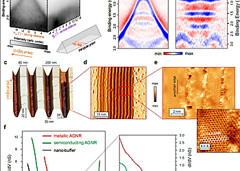
a, 3D photoelectron intensity distribution I(E,θx,θy) mapping the electronic band structure of armchair graphene nanoribbons (AGNRs). The triangular prism sketch represents the overall shape of the electronic structure in a 2D momentum space. The 1D Brillouin zone of AGNRs is oriented parallel to the [112−0]-direction of SiC (i.e., along the ribbons). b, Second derivative plots along the energy axes of high-resolution ARPES spectra measured along and across the ribbons respectively. c, Perspective AFM view of the mesa structures with a periodicity of 200 nm. The trench depth is 20 nm and the facet inclination is around (26 ± 2). d, First derivative of a STM topography image taken on a single facet displaying the “ladder structure” (V = 0.15 V, I = 1.75 nA). e, Magnified view of the mini-facets highlighting the armchair orientation of the sidewall ribbons (V = 2 V, I = 0.5 nA). The inset shows a high-resolution topography image taken on a single ribbon that has a width of about 2 nm equivalent to N ~ 18 dimers. f, STS spectra measured in the center of the ribbons of different widths displaying both semiconducting and metallic behaviors. The inset shows a zoom-in around the Fermi level.
ARPES Measurements
ARPES measurements were carried out at the Bloch beamline of the MAX IV synchrotron facility in Lund, Sweden. High-resolution energy-momentum cuts were measured using a high performance deflector-based DA30 hemispherical analyzer from Scienta Omicron. The energy and angular resolutions were set to 15 meV and 0.1 respectively. The spot-size of the beam measured 10 × 24 µm2, simultaneously probing around 2000 AGNRs. All ARPES data were acquired in ultra-high vacuum (UHV) at a sample temperature of 80 K.
STM/STS Measurements
The STM/STS measurements were performed in UHV (p < 2 x 10-11 mbar) at 80 K using a commercial Omicron LT-STM. The sample was degassed at an elevated temperature of 800 K for several hours before being transferred to the low-temperature chamber. Several electrochemically etched tungsten tips were utilized during the experiments. A lock-in detection technique was used to accumulate and average over 50 STS spectra taken on each individual ribbon.
Authors
Hrag Karakachian, T. T. Nhung Nguyen, Johannes Aprojanz, Alexei A. Zakharov, Rositsa Yakimova, Philipp Rosenzweig, Craig M. Polley, Thiagarajan Balasubramanian, Christoph Tegenkamp, Stephen R. Power, and Ulrich Starke.
Institutes
1) Max-Planck-Institut für Festkörperforschung, Heisenbergstraße 1, 70569, Stuttgart, Germany
Hrag Karakachian, Philipp Rosenzweig & Ulrich Starke
2) Institut für Physik, Technische Universität Chemnitz, Reichenhainer Straße 70, 09126, Chemnitz, Germany
T. T. Nhung Nguyen, Johannes Aprojanz & Christoph Tegenkamp
3) Institut für Festkörperphysik, Leibniz Universität Hannover, Appelstraße 2, 030167, Hannover, Germany
Johannes Aprojanz & Christoph Tegenkamp
4) MAX IV Laboratory, Lund University, Fotongatan 2, 22484, Lund, Sweden
Alexei A. Zakharov, Craig M. Polley & Thiagarajan Balasubramanian
5) IFM, Linköping University, 58183, Linköping, Sweden
Rositsa Yakimova
6) School of Physics, Trinity College Dublin, Dublin 2, Ireland
Stephen R. Power
Name and email of corresponding author
Hrag Karakachian
URL of Institute web-pages
https://www.tu-chemnitz.de/physik/AFKO/index.html.en
https://www.maxiv.lu.se/accelerators-beamlines/beamlines/bloch/
https://www.maxiv.lu.se/accelerators-beamlines/beamlines/maxpeem/

