Electronic Band Dispersion Determination in Azimuthally Disordered Transition-Metal Dichalcogenide Monolayers
Result of the Month
Transition-metal dichalcogenide (TMDC) monolayers are the subject of research world-wide because of their unique electronic and optical properties, bestowing these atomically thin materials with huge potential for application in future nanoscale electronic and optoelectronic devices.
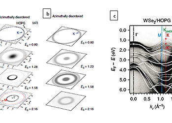
One of the key research targets is understanding the electronic structure of TMDC monolayers in various dielectric environments, because the excitonic nature leads to substantial changes of electronic properties as function of dielectric environment. The most widely used experimental technique to investigate electronic structure – and particularly band dispersion – is angle-resolved photoemission spectroscopy (ARPES), but it is considered to be applicable only to single crystal samples. As most TMDC monolayer samples available today are polycrystalline with random azimuthal orientation of grains, i.e., they are two-dimensional (2D) powders, researchers do not even try to employ ARPES to study these. In turn, this substantially blocks progress.
In our work, we evidence that due to the unique band structure of four different TMDC monolayer materials, it is possible to experimentally determine the band dispersion in the two most important high symmetry directions with high precision using ARPES. By combining experiment with theoretical modeling we rationalize the effect of angular integration for 2D powder samples on general grounds. The experimental work was done using Scienta Omicron instruments at both synchrotron and home lab.
With the information disclosed in our paper, we anticipate that research on TMDCs, also beyond the four prototypical ones covered in our work, will be substantially reinforced, as obtaining detailed insight into the electronic structure of 2D powder semiconductors becomes now possible for a significantly wider range of samples and complex structures.
Authors
S. Park1,2,3, T. Schultz1,2, A. Han4, A. Aljarb4, X. Xu1, P. Beyer1, A. Opitz1, R. Ovsyannikov2, L.-J. Li4,5, M. Meissner6, T. Yamaguchi6, S. Kera6, P. Amsalem1 & N. Koch1,2
Institutes
1) Humboldt-Universität zu Berlin, Institut für Physik & IRIS Adlershof, 12489 Berlin, Germany.
2) Helmholtz-Zentrum für Materialien und Energie GmbH, Bereich Solarenergieforschung, 12489 Berlin, Germany.
3) Advanced Analysis Center, Korea Institute of Science and Technology (KIST), Seoul 02792, Korea.
4) Physical Sciences and Engineering, King Abdullah University of Science and Technology, Thuwal 23955-6900, Saudi Arabia.
5) School of Materials Science and Engineering, University of New South Wales, NSW 2052 Sydney, Australia.
6) Institute for Molecular Science, Okazaki 444-8585, Japan.
Name and email of corresponding author
Prof Norbert Koch, email: nkoch@physik.hu-berlin.de

