Observation of Electrically Tunable van Hove Singularities in Twisted Bilayer Graphene from NanoARPES
Result of the Month
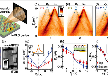
Image Description: Electrostatic tuning of twisted bilayer graphene Dirac cones viewed by nanoARPES. a) Sketch of our nanoARPES experiment with top (red) and bottom (blue) graphene layers contacted by source (S) and drain (D) electrodes and stacked on hBN and on a graphite back-gate (G). A beam of photons is focused to a 690 nm spot using zone plate optics. b,c) Functional region of device presented via optical microscopy (b) and spatially dependent ARPES intensity integrated over E and k (c). The dotted lines demarcate the twBLG flake. d–f) ARPES spectra of the twBLG Dirac cones measured at the given gate voltages. The dashed blue (red) lines represent linearly extrapolated peak positions determined from MDC fits of the bottom (top) layer Dirac cone around KB (KT ) as shown in Figure S3, Supporting Information. g) Gate voltage dependence of n obtained from kF of each Dirac cone. The curves are fits to a linear dependence on gate voltage. The inset presents the resistance of the device measured in situ before exposure to photons. h) Dirac point energies ED determined from the linear extrapolation shown in (d–f) with fits to two separate Vg -dependent functions (curves). The different slopes of the fitted curves in (g,h) result from the smaller amount of charge induced in the top layer (see capacitor model of our device in the inset). i) Demonstration of n-dependence (black curve) of ED for bottom (top) graphene, as expected for non-interacting Dirac cones (see sketch of cones at different doping levels in the inset). The blue (red) markers represent the bottom (top) layer and vertical dashed lines mark the charge neutrality point in (g–i).
Authors
Alfred J. H. Jones, Ryan Muzzio, Paulina Majchrzak, Sahar Pakdel, Davide Curcio, Klara Volckaert, Deepnarayan Biswas, Jacob Gobbo, Simranjeet Singh, Jeremy T. Robinson, Kenji Watanabe, Takashi Taniguchi, Timur K. Kim, Cephise Cacho, Nicola Lanata, Jill A. Miwa, Philip Hofmann, Jyoti Katoch, Søren Ulstrup
Institutes
1) A. J. H. Jones, P. Majchrzak, S. Pakdel, Dr. D. Curcio, K. Volckaert, Dr. D. Biswas, Dr. N. Lanata, Dr. J. A. Miwa, Prof. P. Hofmann, Dr. S. Ulstrup
Department of Physics and Astronomy, Aarhus University, Aarhus C 8000, Denmark
E-mail: ulstrup@phys.au.dk
2) R. Muzzio, J. Gobbo, Dr. S. Singh, Dr. J. Katoch
Department of Physics, Carnegie Mellon University, Pittsburgh, PA 15213, USA
E-mail: jkatoch@andrew.cmu.edu
3) Dr. J. T. Robinson
US Naval Research Laboratory, Washington, D.C. 20375, USA
4) Dr. K. Watanabe, Dr. T. Taniguchi
National Institute for Materials Science, 1-1 Namiki, Tsukuba 305-0044, Japan
5) Dr. T. K. Kim, Dr. C. Cacho
Diamond Light Source, Division of Science, Didcot OX11 0DE, UK
Name and email of corresponding author
Dr. S. Ulstrup
ulstrup@phys.au.dk

