Four Probe Scanning Probe Microscopy
Four Probe Scanning Probe Microscopy (4P-SPM) experiments are performed, when the electrical conductivity of microscopic objects on the nanometer/micrometer scale has to be determined. This method is the microscopic version of 4 probe measurements that are routinely done on a macroscopic scale.
If the electrical resistivity of a macroscopic sample has to be measured the most straight forward method is to use the two contact pins of, for example, a regular multimeter, and measure the voltage drop between those two pins when in contact to sample and use Ohm’s law to calculate the resistivity. When performing this measurement, one measures, however, also the additional contact resistance between the probes and sample; thus, the obtained value is actually incorrect. One way to overcome the intrinsic limitation of the two-probe approach is to separate the voltage and current in the measurement configuration by having two sets of probes: One pair of probes measures the voltage drop - while the other pair injects a current, allowing to calculate the total resistance R of the specimen. In commercially available macroscopic four-probe devices (often used in semiconductor industry), the four probes are aligned along a line at a distance of a few mm. The outer two probes inject the current, while the inner two measure the voltage.
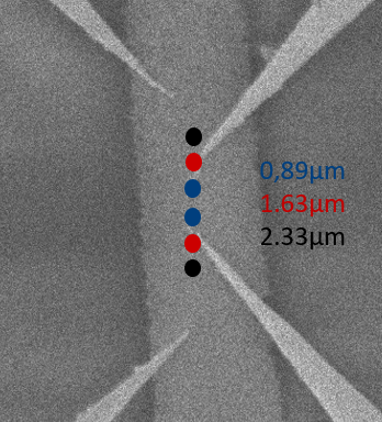
If similar resistivity measurements have to be performed on microscopic samples, it is possible to replace the electrodes or pins (of multimeters) by atomically sharp Scanning Tunneling Microscopy tips. The navigation of the tips and their placement on a microscopic specimen is monitored with a Scanning Electron Microscope.
For a detailed description see: I Miccoli et al 2015 J. Phys.: Condens. Matter 27 223201.


