Manipulation of Fractionalized Charge in the Metastable Topologically Entangled State of a Doped Wigner Crystal
Result of the Month

SEM image of the STM setup and a WS cell construction of the emergent domain wall network. Two outer STM tips (#1 and #2) are jammed into the sample for electrical current sourcing in the lateral direction, tip #3 is used to scan the area in between. The domain structure is schematically indicated with coloured domains (not to scale). The current path is shown schematically with yellow arrows. Zoom-in shows a WS cell construction of the domain wall network induced by the lateral electrical current recorded by tip #3.
We explore the dynamic and microscopic structure of metastable electronic networks in a 1T-TaS2 material, created by surface current injection into the commensurate charge density wave (CDW) ground state. For this purpose, we use multiple independently positioned tips in a low-temperature STM, whose positioning is aided by an integrated scanning electron microscope (SEM). This enables us to mimic a practical device, and for the first time microscopically ascertain the absence of conventional CDW sliding behaviour in response to an electric field at low temperatures. The domain networks created in the current path between two closely spaced STM tip electrodes on the crystal surface are analysed in terms of a Wigner-Seitz (WS) cell construction which enables us to investigate the topological rules and observe charge fractionalization within the networks created by charge injection. Surprisingly, it appears that the effective charge of the electrons in no longer integer, but takes on fractional values such as 13/10, 23/40 and 3611/5000. The number of such fractional states is large, but finite. While the undistorted WS lattice is hexagonal, we find that the emergent domain structure contains defects mostly in the form of pentagon/heptagon pairs. The STM images reveal the formation of two types of defects at the domain wall crossings: trivial defect, where no dislocation is formed in the WS superlattice and their Burger’s vector sum around the vertex is zero; and non-trivial ones, for which a dislocation forms in the WS superlattice with a non-zero Burger’s vector. The non-trivial topological defects at the domain wall junctions- which are homotopically equivalent to crystal dislocations- protect the mesoscopic network structure from external perturbations and are responsible for the non-volatile behaviour of the metastable state at low temperatures.
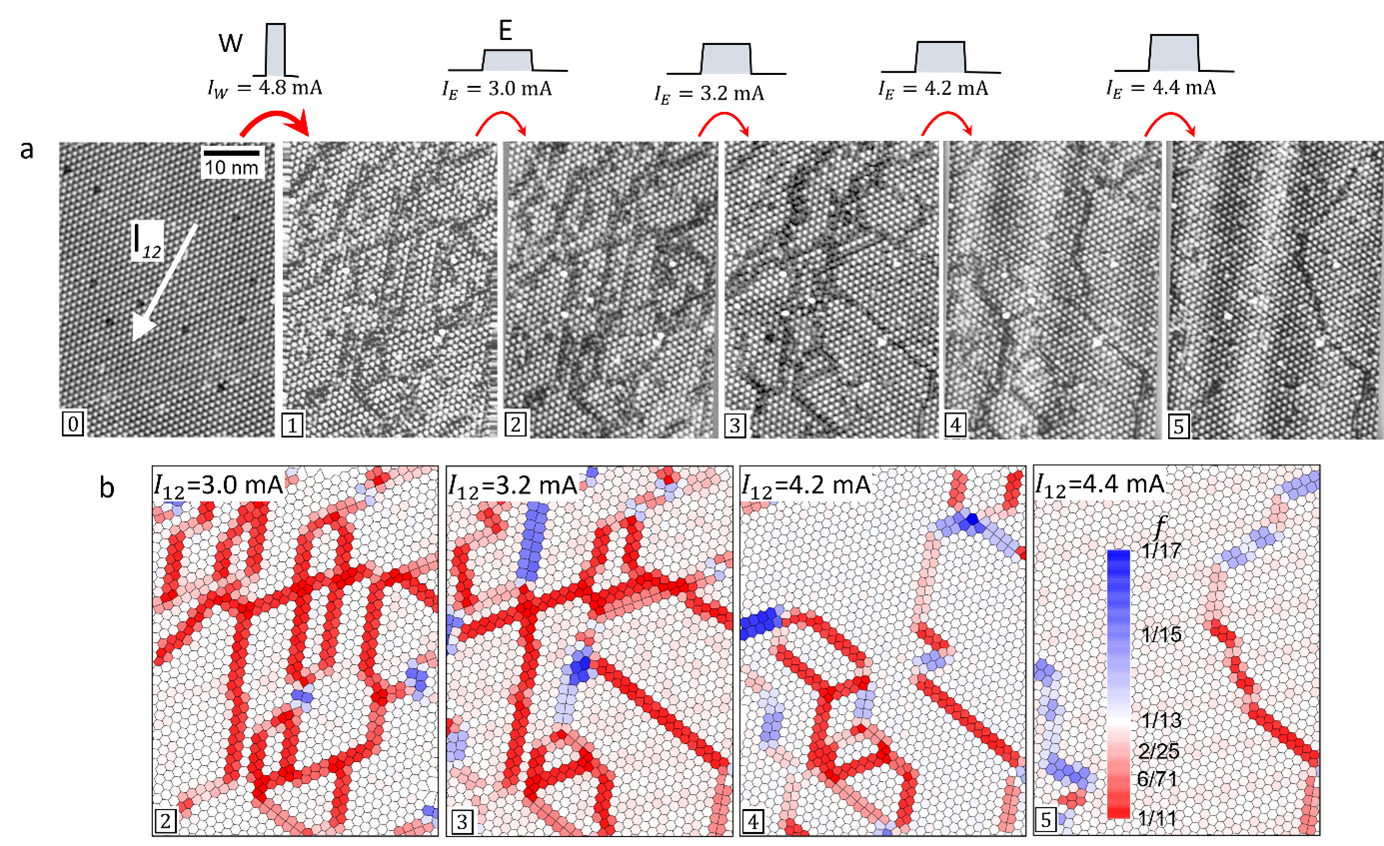
Step by step erase sequence of the domain wall network recorded by the STM in a) and presented as WS cells in b). a) Panel 0 shows the ground commensurate CDW state with the direction of the lateral electrical current marked, and panel 1 is the switched state. Panels 2-5 present part of the erase sequence at higher erase currents that show gradual deletion of the switched domain state. STM imaging was performed in constant current mode with the STM tip biased at -0.8 V with respect to the sample and the tunnelling current set to 1 nA. b) WS cell construction of some of the images in a) with the corresponding panel numbers marked. The commensurate superlattice with undistorted hexagonal cells is seen in white (or near white), while domain walls are mostly red, which indicates a higher current density compared to the commensurate cell. The scale for the filling fraction f is presented in the inset to panel 5.