Talks at APS March Meeting
APS March Meeting is in Las Vegas for 2023. The meeting is organised by the American Physical Society (APS) and is one of Scienta Omicron's most important events during the year. About 12 000 physicists gather for the APS meeting. The event provides a great opportunity for us to connect science with business and to meet our customers in person. This year we will join APS with a commercial booth and also have scientific talks during the week. You can read more about our talks below.
If you are at the APS, come and meet us in booth 501 to learn more and hear about our latest developments!
SCIENTIFIC PRESENTATIONS
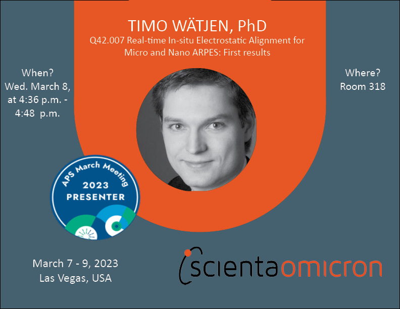
Real-time In-situ Electrostatic Alignment for Micro and Nano ARPES: First results
Presented by Timo Wätjen
Wed. March 8, 4:36 p.m. – 4:48 p.m. PST
Room 318
Abstract:
High quality ARPES measurements, particularly micro/nanoARPES, require highly optimized alignment of the excitation photon beam, sample, and analyzer focal point. Scienta Omicon's new DFS30 spectrometer (patent pending) simplifies this alignment by employing electronic adjustment of the analyzer focal point. In this presentation we will show the first results from our ground-breaking real-time and in-situ Electrostatic 3D Focus Adjustment technology. By replacing imprecise mechanical movements with precise electrostatic adjustments of the lens tables users are able to greatly improve data quality and repeatability in ARPES measurements, as well as providing significantly improved workflow, speed, and reproducibility when optimizing experimental conditions.
Generally ARPES measurements require time consuming, iterative alignment of sample position and light source to match the photoelectron emission spot with the analyzer focal point. Without optimized alignment operation of the analyzer measurement data quality may be compromised. The Electrostatic 3D Focus adjustment technology allows users to generate dynamic lens tables in real time in order to achieve fully optimized deflection, angular and/or transmission modes for data collection. These live lens tables enable calibrated and continuous electronic shifting of the analyzer focal point in three dimensions. This technology represents a major advancement for micro- and nano-ARPES.
As part of our presentation, we will discuss how the alignment of focal point and emission spot is a general ARPES issue, but is particularly important for micro/nanoARPES application as misalignment effects scale with smaller spot sizes and photoelectron kinetic energy. ARPES spectra of graphene measured at the Bloch beamline at MAX IV will be shown as a model case and used as an example to demonstrate the significant impact of the Electrostatic 3D Focus Adjustment on data quality.
More information here.

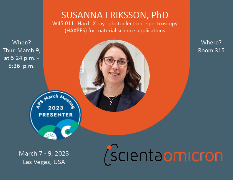
Hard X-ray photoelectron spectroscopy (HAXPES) for material science applications
Presented by Susanna Eriksson
Thu. March 9, 5:24 p.m. – 5:36 p.m. PST
Room 315
Abstract:
Investigating buried interfaces, device electronics or batteries by chemically sensitive instrumentation is highly desired in materials science applications. X-ray photoelectron spectroscopy (XPS) is a powerful method to investigate the chemical nature of surfaces. However, investigations of buried interfaces occurring in, e.g., device electronics are difficult as the energies of the created photoelectrons are not high enough and scattering inside the material’s bulk limit the detected signal intensity. During the past decade, increased attention has been shown to hard X-rays in the photoelectron spectroscopy field. This is primarily due to the increased information depth enabled by the higher photon energies. Using Scienta Omicron’s HAXPES Lab, featuring a monochromatic Gallium K_alpha X-ray source in combination with a hemispherical electron analyzer that includes a +/- 30 degree acceptance angle, we were able to investigate buried interfaces, in-operando devices and real world samples.
In this presentation we will give an overview of applications with a focus on bias-applied measurements from device electronics. Investigating a layered structure of 4 nm thick ZrO2 on 20 nm TiN on p-doped Si, the binding energy shift could be characterized upon applied voltage in-operando without sample destruction. These changes can be assigned to trapped carriers in the defect level at the Ti-N/p-Si interface.
More information about the talk here.


