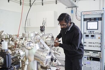
Scienta Omicron’s Products at the CQC2T in Australia
The Atom Fabrication Laboratories at CQC2T were established in 2001 to provide a unique set of facilities for the development of atomically precise devises in silicon. The laboratories house a variety of Scienta Omicron products including a LT NANOPROBE, LT STM and several VT STM Labs. Each of the systems offer both high-quality silicon growth and high-resolution scanning tunnelling microscopy capabilities.
The below text comes from the ARC CQC2T website and describes in more detail how our systems are used for research. Please visit the ARC CQC2T website to find out more about their interesting and important research.
"The majority of work on understanding surface chemistry is performed on a Variable Temperature Scanning Tunneling Microscope (VT-STM) from Omicron Nanotechnology and consists of a custom-configured, triple-chamber UHV STM/MBE system. The STMs can be operated at temperatures ranging from 25 K to 1100 K and a second UHV chamber houses silicon sources for the MBE growth epitaxial silicon with thicknesses up to hundreds of nanometers.
The multi-chamber STM-SEM/MBE system was our first system to undertake qubit fabrication development and provides the necessary registration and high purity silicon growth capabilities required for multi-qubit fabrication. Specifically, the MBE system is capable of device quality Si and SiGe growth wafers up to 4” diameter, with low background doping levels. A low temperature oxide chamber is available for the development of high quality silicon dioxide barrier layers, using resistive silicon sublimation (SUSI) and an RF plasma neutral atomic oxygen source. Operating under UHV conditions, the STM-SEM and MBE chambers are physically connected even though they are housed in different, acoustically shielded laboratories within the AFF. The STM system incorporates an SEM that allows registration markers to be easily found without damaging the STM tip. A specially designed optical position readout system is also incorporated to allow precise alignment of features during successive fabrication steps.
The Omicron Nanoprobe four probe STM system is configured for in-situ electrical characterization of nano- and atomic-scale devices and a separate combined Variable Temperature (VT) STM and a Low Temperature (LT) STM system is used to directly imagine the donor wavefunctions, which when coupled with a Nanonis STM controller from SPECS Zurich allows state-of-the-art spectroscopy."
Read more about our VT SPM, LT STM and LT NANOPROBE through these links.

