HAXPES Lab and what it can do for the electronics industry?
Hard x-ray photoelectron spectroscopy (HAXPES) is an extremely powerful analytical tool for characterizing and understanding materials. HAXPES is a variant of XPS. XPS is a highly surface sensitive technique that utilizes the photoelectric effect to probe the electronic states of a material. A monochromatic photon beam is used to excite electrons within a material, allowing some to escape and become photoelectrons. Their final kinetic energy provides information on elemental composition, atomic charge state, and any other material properties.
Lebens-Higgins, Z.W., et al. Sci Rep 9, 17720 (2019).
XPS measures a material’s occupied electronic states. Core levels provide information on atomic composition and elemental charge states. Valence band provides detailed information on inter-atomic bonding and optoelectronic properties.
Valence bands can have complicated structure due to bonding, hybridization, and other interactions with the neighboring atoms. Semiconductors, materials, etc., have unique signatures in the valence bands. Core level peaks are symmetric for insulators, but asymmetric for metals due to excitation of conduction band electrons.
Looking at HAXPES
Band alignment among materials determines the behavior of devices. Valence band can be used to determine band alignment of materials. XPS is a powerful technique. Different photon energies result in different photoelectron escape depths. Here, HAXPES comes into the picture. High-energy x-rays can access tightly electrons much deeper inside a sample. HAXPES uses high energy, synchrotron x-ray radiation giving probing depths in tens of nms.
Looking at benefits of HAXPES, real devices are composed of multiple buried material interfaces. XPS is a surface science technique. Probing beyond the surface with HAXPES allows us to study subsurface regions, including buried device interfaces.
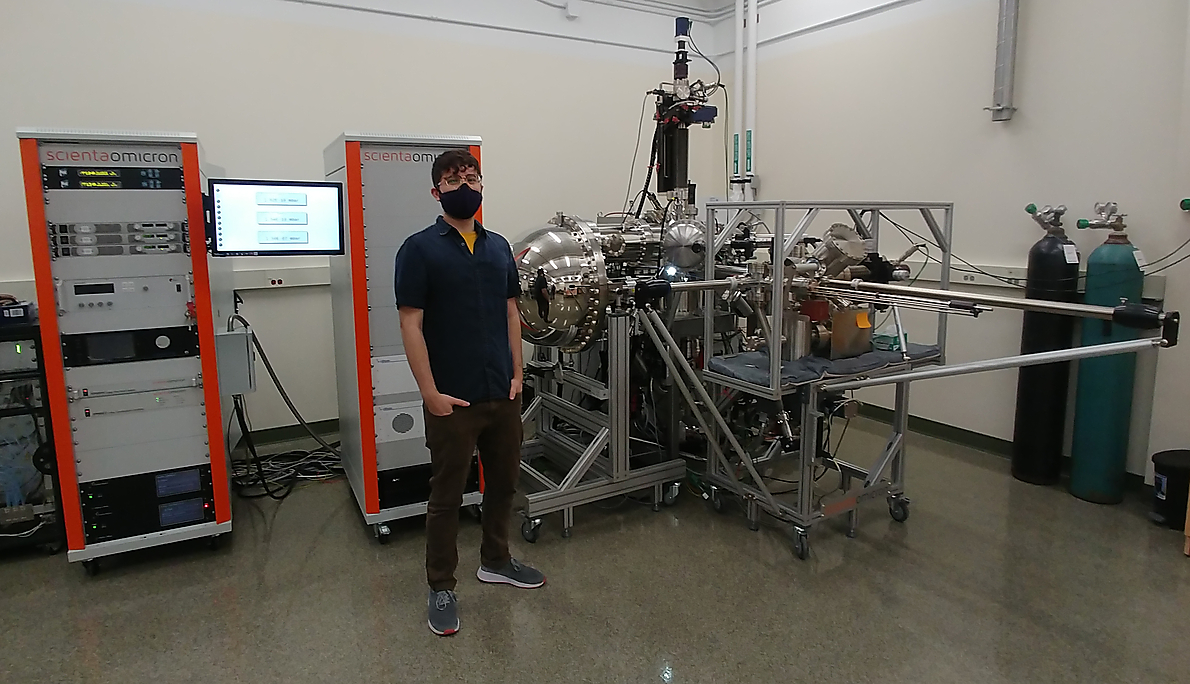
The Scienta Omicron HAXPES Lab is a small lab-based system that provides synchrotron-comparable HAXPES spectra. The system at Binghamton is the first lab-based Ga-Kx HAXPES in the USA. The 9.2 keV x-rays produced by the Ga jet source can probe up to 60nm deep. This can circumvent surface contamination and the overlayers.
We need to look at the Metaljet x-ray source. Solid anodes have limited brightness due to material limitations. We can use an anode that has already melted, e.g., liquid metaljet of gallium. The Excillum Metaljet source uses a laminar flow of liquid Ga/In alloy as the x-ray generating anode. This enables rapid removal of excess heat from the anode, allowing for high brightness without melting.
The brightness, small spot size, and high resolution of the lab-based HAXPES makes it ideal for investigating complex systems, such as real-world microelectronic devices. The Excellium Metaljet source provide a massive increase in brightness over traditional lab-based x-ray sources. This drastically reduces the time it takes to acquire usable, lab-based HAXPES spectra, making it more comparable lab-based XPS systems, and even more HAXPES beamlines.
The brightness, small spot size of 35 microns in diameter, and high resolution of the lab-based HAXPES make it ideal for investigating complex systems, such as real-world microelectronic devices. HAXPES Lab utilizes the same hemispherical analyzer as some synchrotron HAXPES beamlines. The analyzer provides excellent energy resolution.
What can you do with HAXPES Lab?
We investigate the electronic structure and properties of materials. HAXPES Lab can perform non-destructive depth studies using traditional Al-Kα source along with Ga-Kα source. HAXPES Lab at Binghamton is equipped with a sample preparation chamber and an inert transfer system.
Samples can be mounted in an Ar glovebox and transferred to the system using vacuum suitcase. Standard SHOM style plates are used to mount samples up to 10 x 10 mm. Sample heating can be done in the preparation chamber. Sample heating/cooling can be done in the main chamber. You can do heating/cooling during HAXPES measurement. The temperature-dependent XPS/HAXPES provides information on the evolution of the electronic structure during SPTs, MITs, thermal decay, etc.
Operando measurements can be performed on electronic devices using SHOMDC sample plates. Device terminals can be connected to the sample plate rails via wire bonding, spot welding, etc. HAXPES Lab manipulators have brush contacts for biasing. The sample plate itself can act as a third electrical contact or ground. Two- or three-terminal devices can be potentially investigated at HAXPES Lab.
Relative sensitivity factors (RSFs) are necessary for quantitative XPS/HAXPES measurements. As of now, RSFs cannot be reliably determined for variable energy synchrotron-based HAXPES. RSFs depend on photon energy. It has to be reliable specific energy. Using the Ga-Kα source, a library of core levels for elements up to Z=99 up to a binding energy of 9 keV has already been computed with ratification of values undergoing. HAXPES Lab can also do sputter depth profiling and charge neutralization.
External users can also gain access to the HAXPES Lab.
-
“The post was originally published by Mr. Pradeep Chakraborty.”