Directional picoantenna behavior of tunnel junctions formed by an atomic-scale surface defect
Result of the Month


Atomic defects at STM junctions create picoantennas with directional emission. The image shows an illustration of the directional profile of the light emitted when the STM tip is located over an atomic height step. We have fabricated a picoantenna by approaching a metal tip to a plasmonic surface close to a naturally occurring atomic-scale defect known as a step edge. We demonstrate that, by injecting current through the created tunnel junction, we can excite the plasmonic modes of the picocavity, and the radiation arising from their radiative relaxation can be observed in the far field. By studying step edges with different orientations, we demonstrate that the light emission is directional and, thus, that such picocavity acts as a picoantenna, opening new avenues to control light-matter interaction at atomic scales.
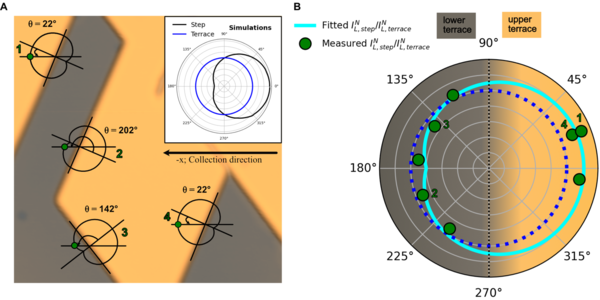
Directionality of plasmonic emission for picoantennas formed by a monoatomic height step. (A) STM image of a Ag(111) surface with steps at different orientations. STM image acquisition settings: size = 25 nm x 25 nm, Isp = 10 pA, Vsp = 1.0 V. The angles formed between the line perpendicular to each step and our collection direction (-x) are annotated. Inset: EM simulations of the integrated light emission when the tip (sphere) is placed 0.35 nm away from a monoatomic height step (black curve), and over the flat terrace (blue curve), as a function of the azimuthal angle in polar coordinates. (B) Angular distribution of the normalized light (divided by the normalized light at the terrace for comparison with EM simulations). The green dots labeled from 1 to 4 correspond to the integrated normalized light intensity when the STM tip is located near the steps marked in (A), referred to each step’s frame of reference, where the upper terrace is at the right (orange shaded background), and the lower terrace is at the left (gray shaded background). The experimental data as a function of the azimuthal angle defined by the orientations of the steps do not follow a circumference, blue dotted circle representing isotropic emission, implying directional emission. The cyan line is a fitting of our experimental data to a cardioid-like function. The non-labeled green dots are experimental data at other angles obtained by rotating the sample.
Dr. Alberto Martin-Jimenez adds "Combining the Scienta Omicron LT STM with my optical setup has been highly effective for my research. The STM’s precision and stability make it an excellent platform for studying nanoscale light-matter interactions, enabling reliable and high-quality experiments that advance our understanding in this field."