Efficient, Non-Destructive Characterization of Buried Layer Chemistry

Ask the Experts Seminar
Buried layers and their interfaces play a critical role in the performance of devices such as batteries, solar panels, and transistors. Accurately analyzing the chemistry of these inner layers is essential for advancing materials and improving device functionality. However, accessing these regions non-destructively remains a significant challenge. Traditional X-ray Photoelectron Spectroscopy (XPS) is a trusted tool for surface analysis, but its limited probing depth makes it unsuitable for exploring deeper layers without damaging the material.
This is where Hard X-ray Photoelectron Spectroscopy (HAXPES) provides a compelling advantage. With its ability to probe further below the surface non-destructively, HAXPES has emerged as a powerful technique for investigating complex materials, including thin films, semiconductors, metals, and coatings.
In this interactive seminar, we will demonstrate how HAXPES enables deeper insights into buried interfaces and oxidation processes in real-world devices. Through practical case studies—including research on semiconductor devices, optical thin film interfaces, and band structure changes in MOS structures—you'll discover how HAXPES is pushing the boundaries of modern materials analysis.
Key learning objectives
- Understand the key advantages of Hard X-ray Photoelectron Spectroscopy (HAXPES) compared to traditional XPS for non-destructive analysis of buried interfaces and deeper layers in complex materials.
- Gain insight into practical applications of HAXPES through recent research examples, including semiconductor devices, optical thin film interfaces, and MOS structures.
- Identify how HAXPES can provide critical information about oxidation states, interface chemistry, and electronic band structure in technologically relevant devices.
- Interact directly with our leading experts to ask questions, clarify doubts, and discuss specific analytical challenges relevant to your research.
Who should attend this webinar
- Material scientists and engineers involved in research and development of thin films, semiconductors, batteries, solar cells, and advanced coatings.
- Analytical chemists and physicists interested in advanced surface and interface characterization methods.
- Researchers and students seeking to deepen their understanding of cutting-edge characterization techniques in materials science.
- Industry professionals looking for innovative methods to improve product performance and quality through enhanced materials analysis.
Meet the speakers

Dr. Tamara Sloboda
Product Manager, HAXPES & XPS
Dr. Sloboda holds a PhD in Chemistry from KTH – Royal Institute of Technology where she investigated chemical and electronic properties of quantum dot and perovskite photovoltaics using synchrotron-based photoelectron spectroscopy. After this, she joined Scienta Omicron in 2023 as a Product manager for products in HAXPES and XPS field, this way maintaining a strong focus on customer needs and product development. She is currently involved in several instrument developments and is supporting related activities to ensure alignment with ongoing project goals and timelines.

Dr. Marcus Lundwall
Director of Development, Industrial Applications
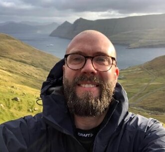
Dr. Lundwall holds a PhD in Physics from Uppsala University, where his research focused on the creation and structural characterization of nanoparticles using synchrotron-based electron spectroscopy. He joined Scienta Omicron in 2007 as a Technical Sales Engineer and has since held key positions in both R&D and business unit management, consistently maintaining a strong customer focus. Among his contributions, he played a central role in the development and launch of the EW4000 analyzer and the monochromated 9.25 keV X-ray source, both of which are integrated into the HAXPES Lab system. He currently leads instrument development for industrial applications.
