Copper Clusters on h-BN-Covered Pt(110): Nucleation, Stability, and Local Surface Potential
Result of the Month
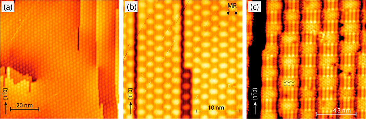
Figure 1. Same surface, different views: STM images of hexagonal boron nitride monolayers on Pt(110). (a) The large-scale Moiré pattern of h-BN extends over steps and screw dislocations. (b) Close-up view of the Moiré pattern. The alternating (1 × 5) and (1 × 6) missing-row structure of the underlying Pt surface layer is resolved. According to DFT-based STM simulations, the bright regions of the Moiré correspond to regions with N atoms close to on-top positions, while regions with B atoms close to on-top positions are imaged darker. (9) (c) Atomically resolved STM image: In the bright areas of the superstructure the honeycomb-lattice due to the h-BN overlayer is observed as indicated by the schematic model superimposed in one of the bright regions. The dark domains oriented along [110] as visible in the bottom center of (b) and on the left side of (c) are due to a nonperfect terrace structure of the Pt substrate, probably caused by nonperfect healing of the (reconstructing!) surface during hBN growth.
In this paper we explore the effect of this geometrically and electronically complex superstructure on the adsorption of foreign atoms/molecules by investigating nucleation, growth, and stability of copper clusters on h-BN/Pt(110). In particular we answer the following questions: (i) Where does nucleation occur preferentially? Are the regions above the missing Pt rows more inert with respect to nucleation and adsorption of copper? Does nucleation/adsorption differ on regions where N atoms are located close to on-top positions from nucleation/adsorption on regions with B atoms in on-top positions? (ii) What happens when the clusters grow in size? Do the missing rows limit lateral growth; that is, can the surface be used to grow nanowire arrays? (iii) Are flat, monolayer thick Cu nanostructures formed, or does 3-dimensional growth prevail already at small coverages (wetting behavior)? (iv) As Pt(110) is close to a tipping point with respect to surface reconstruction, does Cu adsorption on the h-BN film possibly cause restructuring of the underlying Pt(110) surface? (v) Are the copper structures thermally stable? Can one achieve or avoid, intercalation of copper between the platinum substrate and the h-BN overlayer, respectively? (vi) Finally, how are the electronic properties of Cu clusters, for example, the local surface potential (viz. “local work function”), of copper clusters modified by the h-BN/Pt template?
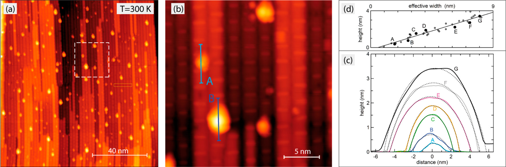
Figure 2. (a) STM image taken after deposition of small submonolayer amounts of Cu (∼0.05 ML) onto h-BN/Pt(110), followed by warming to 300 K. (b) Magnification of the square region indicated in the central part of (a). (c) Height profiles. A and B are from the 0.05 ML experiment of (b), while profiles C–G are from annealing experiments with a larger initial coverage (∼1.5 ML; for images see Figure 3). The thin dashed lines are fits with a spherical-cap model. (d) Profile height versus effective width. The latter is defined as the area under the profile curve divided by its height and is close to the full width at half-maximum. Large filled circles correspond to the profiles shown in (c), while small open circles are from cluster profiles not shown in the article.
Experiments were performed in an ultrahigh-vacuum two-chamber setup INFINITY SPM Lab from Scienta Omicron (base pressures ≈2 × 10⁻¹⁰ mbar), consisting of a chamber for sample preparation and a separate one for performing STM measurements at low temperature (8 K). The sample was transferred between both chambers with a magnetically operated transfer rod.
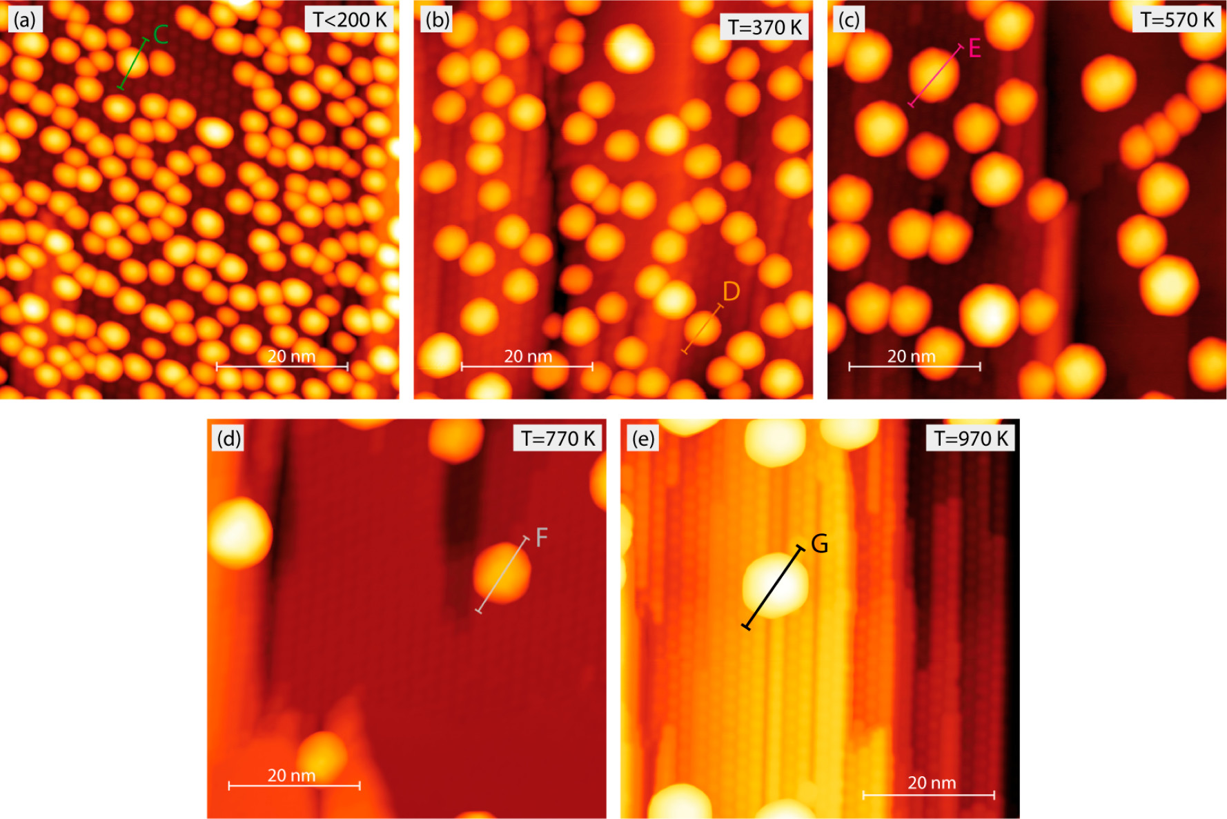
Figure 3. STM images of Cu clusters on h-BN/Pt(110) after annealing to different temperatures. Initially ∼1.5 monolayers of copper were evaporated onto the surface.