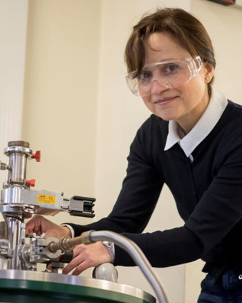
Atomic Layer Semiconductors Poised to Change Our Lives
Amalia Patanè is Professor of Physics and Director of Research at the School of Physics and Astronomy at the University of Nottingham. For the last few years, she has been working on van der Waals crystals. These are extremely thin crystals, made up of atomically thin layers. These layers are not bound by ordinary covalent bonds, like in traditional semiconductors, but by much weaker van der Waals bonds.
"That makes it much easier to make extremely thin layers, on the scale of a few atomic layers", Professor Patanè says. "This creates a plethora of opportunities for science and technology. New quantum properties emerge at the atomic scale; the layers can be bent; they can be combined together without the limitations that apply to conventional semiconductors. Also, they can be rotated relative to each other, and by twisting them it is possible to create new crystal structures."
This means that these materials may hold the key to "post-silicon" electronics.
Much of today's electronics are based on the ubiquitous semiconductor. These are used to build integrated circuits ("computer chips"), CCD's in cameras, diodes such as LEDs that are increasingly dominating lighting, and in many other applications.
A key task for science has been to shrink the size of integrated circuits and other semiconductor arrays so that they can be used in new types of devices, whilst increasing the power and utility of existing devices.
"Science has been incredibly successful at this, but we are now approaching hard, physical limits", says Professor Patanè.
The 2D semiconductors that she and her colleagues are working on represent a very promising way forward. They may transform many of the technologies we see around us and use every day, with applications in computing, energy, medicine, communications, lighting and other fields. Digital electronics built with 2D semiconductors will require less power. 2D semiconductor solar cells will be more efficient. Drugs may be delivered with greater precision, and there may be applications in quantum computing, nanoelectronics and optoelectronics.
However, the road forward is not without its roadblocks.
"The problem with atomically thin van der Waals crystals is that we don't know how to make them. Up until now, we have started with a bulk crystal and shaved away layers mechanically, usually using Scotch tape!"
Of course, this technique cannot be used if these materials are to be produced on an industrial scale. Another problem is that there is really no way to dope the materials or modify their composition – to introduce and create tailored physical effects.
"This ability to modify the composition of the crystal is essential for future discoveries and technology applications. And we don't yet know how to do it."
Amalia Patanè and a diverse group of specialists across many countries are working to change this.
"In 2019, my colleagues and I developed an ambitious plan for a bespoke facility to synthesise these materials with atomic precision, and to see and manipulate their quantum properties. We were later awarded three million euros from UK Research and Innovation and the University of Nottingham to build the new facility, which we plan to install at Nottingham in April 2021. It's all very exciting."
The Nottingham team has named this new facility EPI2SEM (EPItaxial growth and in-situ analysis of 2-dimensional SEMiconductors).
"Now we will be able to actually control the composition, and to develop new materials by building them atom by atom. It will be a vast improvement on the sticky tape approach", she says, smiling.
It wasn't set in stone that Amalia Patanè would end up in physics. She had many strings to her bow when in high school. Almost literally.
"I played piano since I was six and learnt to play violin later. And my music teacher of course wanted me to pursue my passion for piano. One teacher wanted me instead to become a medical doctor, which my mother also wanted. But I thought there was a beauty in physics. So that’s what I chose."
She had a broad interest in science, and chose between mathematics, chemistry and physics.
"At seventeen, chemistry felt too dirty", she says, "and mathematics felt too dry. With physics I got everything, so that's where I ended up. I liked the idea of trying to understand the laws of nature. But I still like playing the violin and piano."
Different things have been in focus at different stages of Professor Patanè’s career. She feels that her focus has widened from her own research in quantum physics.
"My own research is still especially important, of course. But as I've progressed with my career, I have been taking responsibilities for others. Promoting the science of colleagues and research students is an essential part of my daily job. As a Director of Research, I oversee the School's research and its future development. Also, I lead international projects. Since 2015, I coordinate UK membership of the European Magnetic Field Laboratory (EMFL), which is available as a National Research Facility to the whole UK research community working in many fields of science. So, what has been important for me has changed over the years."
Professor Patanè is leading the EPI2SEM project.
"It is an exciting opportunity, not only for me, but for my colleagues, and for our many international partners. EPI2SEM would not have been possible without the support from colleagues with expertise in many different fields. Science really does not know national boundaries. We need to find the best groups and people in the world to reach important goals like this for the benefit of all."
Professor Amalia Patanè
Professor of Physics and Director of Research, Faculty of Science
Contact
Telephone: 0115 951 5185
Email: amalia.patane@nottingham.ac.uk
Article written by:
Kim Bergström - Science Journalist - Ord & Vetande

