Photodriven Transient Picosecond Top‐Layer Semiconductor to Metal Phase‐Transition in p‐Doped Molybdenum Disulfide
Result of the Month
Figure Description
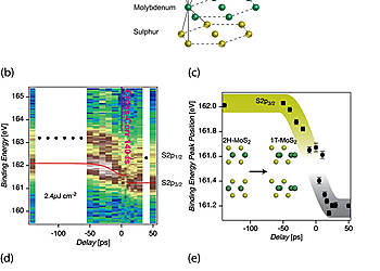
2H‐semiconductor to 1T‐metal top layer phase transition in p‐doped bulk 2H‐MoS2 from time‐resolved ESCA: a) The principle of time‐resolved ESCA: optically pumped bulk p‐doped 2H‐MoS2 probed by X‐ray photoelectron spectroscopy at the S2p core levels with an angle‐resolved time‐of‐flight (ArTOF) electron spectrometer. b) Femtosecond time resolved S2p core level lines at 140 fs X‐ray/optical cross‐correlation (red line guide to the eye of experimental peak position). c) Temporal evolution of S2p3/2 peak positions (as resulting from a single‐component Gaussian fit) using the spectra from (b) shows the surface photovoltage shift and a fast phase transition. d) Picosecond time‐resolved S2p core‐level lines at 50 ps X‐ray/optical cross‐correlation. The S2p multiplet shifts to lower binding energy when approaching the temporal overlap. e) Center of mass (CoM) position of the S2p3/2 core level and width. The large increase in the peak width is revelatory of the 2H to 1T phase transition; the CoM peak position reflects the dynamics of both, the phase transition and the SPVS.
Author´s Note
In this work, we establish how visible light itself can create a transient metallic top layer on bulk crystalline p‐doped 2H‐MoS2. Electron–hole pairs created by optical excitation separate in the surface band bending region of p‐doped semiconducting 2H‐MoS2. This causes a transient accumulation of electrons in the surface region, driving the top‐layer within several picoseconds from the p‐doped semiconducting 2H‐MoS2 into a sheet of metallic 1T‐MoS2 at a remarkably low optical fluence threshold. This mechanism has significant implications on how optically illuminated MoS2 surfaces behave, and will positively change the catalytic properties for water splitting.
Experiment
The experiments were performed at the Plane Grating Monochromator (PGM) branch of the “FemtoSpeX” facility at Bessy II (UE56/1‐PGM) using the “FemtoSpeX Molecules and Surfaces” endstation. The monochromator was equipped with three gratings: 1200 lines mm−1, 400 lines mm−1, and 150 lines mm−1. The regular fill pattern of BESSY II consisted of several parts: The multibunch part, with 2 ns spacing between consecutive bunches, an ion clearing gap of 200 ns, and several isolated bunches with a higher current. Two of these isolated bunches were located within the ion clearing gap and one of them was excited by a radio transmitter effectively allowing single bunch operation at the endstation. This method is called pulse picking by resonant excitation (PPRE). The remaining isolated bunches were located in the multibunch part and were dedicated to the femtosecond slicing process. The strength of this beamline was thus the availability of regular single pulse synchrotron radiation (50 ps FWHM) and femtosecond X‐ray pulses (≈120 fs FWHM) with variable polarization by tuning the electron beam and beamline optics. The 150 lines mm−1 grating was used for the measurements using the femtosecond X‐ray pulses, yielding a resolution of E/ΔE ≃ 103 and the 1200 lines mm−1 grating for the picosecond measurements. A photon energy of 260 eV and vertical polarization were used. Combining the pulses delivered by the synchrotron, a synchronized femtosecond optical laser available at the beamline and a high transmission angle‐resolved time‐of‐flight electron spectrometer (ArToF) with an acceptance of 56° enabled the investigation of the dynamics of core levels.
Authors:
Nomi L. A. N. Sorgenfrei, Erika Giangrisostomi, Raphael M. Jay, Danilo Kühn, Stefan Neppl, Ruslan Ovsyannikov, Hikmet Sezen, Svante Svensson, Alexander Föhlisch
Affiliations:
Dr. N. Sorgenfrei
Institut für Physik und Astronomie Universität Potsdam, Karl-Liebknecht-Straße 24/25 14476 Potsdam Germany
Current address: Institut für Methoden und Instrumentierung der Forschung mit Synchrotronstrahlung Helmholtz-Zentrum Berlin für Materialien und Energie GmbH Albert-Einstein-Str. 15 12489 Berlin Germany
Email Address: nomi.sorgenfrei@helmholtz-berlin.de
Dr. E. Giangrisostomi, Dr. S. Neppl, Dr. R. Ovsyannikov, Dr. H. Sezen
Institut für Methoden und Instrumentierung der Forschung mit Synchrotronstrahlung Helmholtz-Zentrum Berlin für Materialien und Energie GmbH Albert-Einstein-Str. 15 12489 Berlin Germany
Dr. R. Jay
Institut für Methoden und Instrumentierung der Forschung mit Synchrotronstrahlung Helmholtz-Zentrum Berlin für Materialien und Energie GmbH Albert-Einstein-Str. 15 12489 Berlin Germany
Current address: Department of Physics and Astronomy Uppsala University 75120 Uppsala Sweden
Dr. D. Kühn
Institut für Physik und Astronomie Universität Potsdam, Karl-Liebknecht-Straße 24/25 14476 Potsdam Germany
Prof. Dr. S. Svensson
Department of Physics and Astronomy Uppsala University Box 516 75120 Uppsala Sweden, Institut für Methoden und Instrumentierung der Forschung mit Synchrotronstrahlung Helmholtz-Zentrum Berlin für Materialien und Energie GmbH Albert-Einstein-Str. 15 12489 Berlin Germany 1 2 DECAY
Prof. Dr. A. Föhlisch
Institut für Physik und Astronomie Universität Potsdam, Karl-Liebknecht-Straße 24/25 14476 Potsdam Germany Institut für Methoden und Instrumentierung der Forschung mit Synchrotronstrahlung Helmholtz-Zentrum Berlin für Materialien und Energie GmbH Albert-Einstein-Str. 15 12489 Berlin Germany
Corresponding Author:
Dr. N. Sorgenfrei

