Laboratory Based Hard X-ray Photoelectron Spectroscopy for Buried Interface Analysis of Microelectronic Components
Result of the Month
The discovery of the ferroelectricity in silicon-doped hafnium oxide offered the possibility for the integration and scalability of ferroelectric based devices, allowing a CMOS compatible, 3D integration via the well-developed atomic layer deposition (ALD) technique. The single-phase, solid solution Hf0.5Zr0.5O2 (HZO) is a promising material for ferroelectric capacitor integration in 1T-1C memory cells, thanks to its low crystallization temperature, fully compatible with back end of line technology.
The maximum ferroelectric polarization is obtained for a film thickness ~ 10 nm. The formation of chemically distinct interface layers, with distinct electric properties with respect to the HZO can therefore play an important role in ultimate device performance. For example, an interface layer may destabilize the ferroelectric state in the HZO, favour leakage by modifying the Schottky barrier height or reduce the total capacitance of the stack.
Understanding these issues requires techniques capable of accessing the buried interface in a non-destructive manner. HAXPES is the ideal tool allowing to probe the physical chemistry and electronic structure of buried interface layers, providing key information such as the depth profile of oxygen vacancies or the oxidation state of the interface layer.
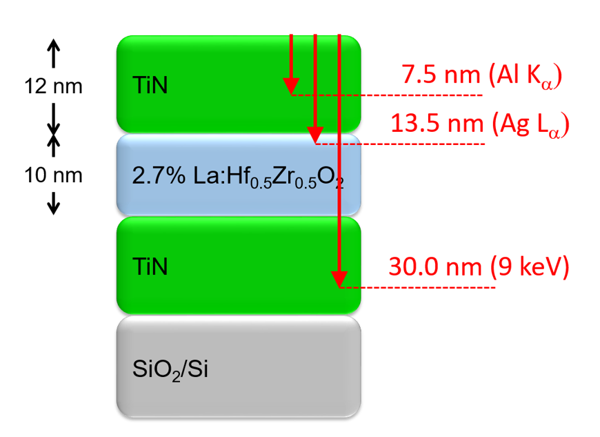
We have used one such sample to benchmark the performance of the laboratory HAXPES system with respect to a typical synchrotron radiation HAXPES set-up. The sample was a 12 nm TiN/10 nm La:HfZrO2/12 nm TiN/SiO2/Si, shown in Fig. 1.

Figure 1 Schematic of 12 nm TiN/10 nm La:HfZrO2/12 nm TiN/SiO2/Si test sample. The approximate probing depths (approximately three times the inelastic mean free path) of Hf 3d electrons excited by Al Kα, Ag Lα and Ga Kα are shown by the red arrows.
The HZO was grown at NaMLab (Dresden, Germany) in an ALD reactor (Oxford Instruments OpAL) at 300 °C using TEMAHf [Hf(N(CH3)(C2H5))4] and Zr[N(C2H5)CH3]4 organic precursors for Hf and Zr, respectively, while ozone was used as an oxygen precursor. The bottom and top TiN electrodes were grown by physical vapor deposition (PVD) sputtering. To order to stabilize the polar orthorhombic phase (Pca21), the sample was annealed for 20 s at 600 °C in nitrogen atmosphere after the top electrode deposition.
The synchrotron HAXPES experiments were done at the BL15XU beamline at Spring8 (Japan) using 8 keV photons and a Scienta R4000 analyzer. The HAXPES-Lab measurements were done using the 9.25 keV Ga Kα1 source and Scienta Omicron EW4000 analyzer.
Identical dwell times, energy steps, spectral ranges, incidence and detection angles where used for both experiments in order to eliminate geometrical effects. Only the number of scans per spectrum was varied in order to obtain reasonable signal to noise ratio and the energy resolution of the analyser were varied.
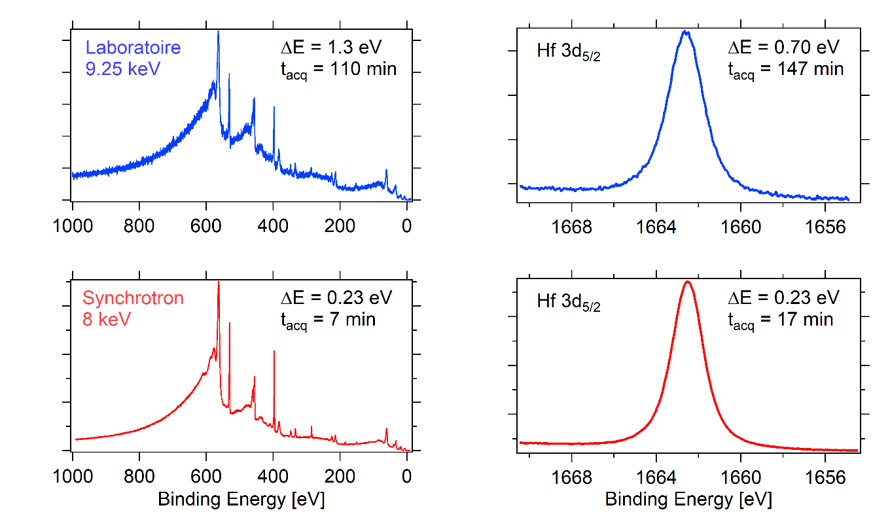
The survey spectra and the Hf 3d5/2 core levels from the synchrotron (red) and laboratory (blue) experiments are reported in Fig. 2 together with the total acquisition time and the spectrometer resolution.

Figure 2 Survey (left) and Hf 3d5/2 core level (right) spectra obtained using laboratory based HAXPES (top) and synchrotron radiation (bottom). For each spectrum, the energy resolution and the total acquisition time are indicated.
The S/N ratio of the synchrotron measurements is better. There is also a factor 3 in energy resolution and a factor 8 in total acquisition tie, with respect to the laboratory HAXPES. However, the full-width half-maximum of the Hf 3d5/2 peak only broadens from 1.84 to 2.00 eV for the laboratory spectrum, quite sufficient to identify subtle changes such as the Hf4+ to Hf3+ ratio, a signature of the oxygen vacancy concentration. The increase in acquisition time is not a major disadvantage given the high stability of the Ga Kα1 source (greater than three days). The 0.7 eV resolution in the laboratory is also sufficient for most analyses of the interface chemistry and band line-up.
Acknowledgements:
This project received funding from the European Union’s Horizon 2020 research and innovation programme under Grant Agreement No. 780302 3eFERRO. The measurements at BL15XU of SPring-8 were performed under the approval of the NIMS Synchrotron x-ray Station (Proposal No. 019A4909). This work was partly supported by the NIMS microstructural characterization platform as a program of the “Nanotechnology Platform” (Project No. 12024046) of the Ministry of Education, Culture, Sports, Science and Technology (MEXT), Japan. The Lab-HAXPES measurements were supported by the CNRS.
Authors:
W. Hamouda,1 C. Lubin,1 S. Ueda,2,3 Y. Yamashita,3,4 O. Renault,5 F. Mehmood,6 T. Mikolajick,6 U. Schroeder,6 R. Negrea,7 and N. Barrett1,8
Affiliations:
1 SPEC, CEA, CNRS, Universite Paris-Saclay, CEA Saclay, 91191 Gif-sur-Yvette, France
2 Synchrotron X-ray Station at SPring-8, National Institute for Materials Science, Sayo, Hyogo 679-5148, Japan
3 Research Center for Advanced Measurement and Characterization, NIMS, Sengen, Tsukuba 305-0047, Japan
4 National Institute for Materials Science, International Center for Materials Nanoarchitectonics, 1-1 Namiki, Tsukuba 305-0044, Japan
5 University Grenoble Alpes, CEA, LETI, F-38000 Grenoble, France
6 NaMLab gGmbH/TU Dresden, N€othnitzer Str., 64a, 01187 Dresden, Germany
7 National Institute for Materials Physics, 077125 Bucharest-Magurele, Romania
8 Fédération de Recherche N° 2050 CNRS SPE- Spectroscopies de Photoémission
Corresponding Author:
Nick Barrett
Email: nick.barrett@cea.fr
Nanostructure Studies and Surface Imaging Laboratory (LENSIS)

