Imaging the Acceptor Wave Function Anisotropy in Silicon
Result of the Month
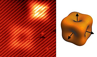

STM image revealing two hydrogenic acceptor states arising from defects beneath a hydrogen-terminated Si(001) surface, exhibiting a characteristic square ring-like contrast superimposed on the atomic lattice (left). Image parameters: 900 mV, 100 pA, 14 x 14 nm2 (z-range 120 pm). This is compared with an isosurface of the corresponding acceptor wave function calculated using the multiband effective-mass approximation (right), which captures the extended, fourfold-symmetric spatial structure of the state.
Understanding the spatial structure of the quantum states associated with individual dopants in silicon is a central challenge for scalable, atomic-scale semiconductor quantum device engineering. While donor wave functions in silicon have been imaged previously, direct visualization of acceptor states has remained elusive. Here, scanning tunnelling microscopy (STM) is used to image hydrogenic acceptor wave functions in silicon for the first time, revealing striking, highly anisotropic square ring-like features extending over ~10 nm and originating from defects buried beneath the Si(001) surface.
The acceptor states are created by high-energy bismuth implantation followed by annealing, producing a p-type surface decorated by individual acceptor defects. Atomic-resolution STM and spatially resolved tunnelling spectroscopy demonstrate that these features arise from neutral acceptor states located approximately 30 meV above the valence band edge. The observed anisotropy and symmetry are reproduced quantitatively by both multiband effective-mass theory and atomistic tight-binding Green’s function calculations, which show that the square-ring appearance originates from the fourfold-degenerate ground-state multiplet of a hydrogenic acceptor and the interplay of light- and heavy-hole bands in silicon.
This work complements seminal STM experiments imaging and spectroscopically probing acceptor states in III–V semiconductors, as well as more recent studies resolving valley-orbit interference in donor states in silicon. Such understanding is critical for the deterministic placement and coupling of acceptor-based quantum states, and for extending atomic-scale quantum device concepts beyond donor-only architectures.
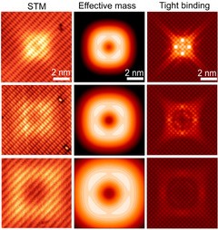
Comparison of experimental STM images (left) with multiband effective-mass simulations (centre) and atomistic tight-binding calculations (right) for hydrogenic acceptor states in silicon. The STM images (top to bottom) were acquired at 1.1 V, 20 pA (z-range 160 pm); 1.6 V, 20 pA (z-range 30 pm); and 1.0 V, 5 pA (z-range 100 pm). Effective-mass contour plots correspond to acceptors located 2.9, 3.9, and 5.9 nm below the image plane, while the tight-binding simulations show topographic maps of the acceptor local density of states at depths of 0.81, 1.62, and 2.17 nm beneath the surface. Both simulated datasets use a colour scale spanning 80 pm. Figure reproduced from Siegl et al., Nano Letters 25, 13996–14001 (2025), licensed under CC-BY 4.0.