Atomic-Scale Thermopower in Charge Density Wave States
Result of the Month
Here, we report on the atomic-scale investigation of thermopower and phonon puddles in the CDW states of 1T-TaS2 using SThEM. In previous studies, large thermopower has been observed at the device scale in the commensurate CDW phase in 1T-TaS2, which is promising for space applications with radiation hardness. In our study, the Star-of-David (SoD) clusters of tantalum and sulfur atoms exhibit drastic and counterintuitive variations in thermopower (4 mV) over a distance of 1 nm. Moreover, in contrast with former scanning tunneling microscopy (STM) studies, the spatial variation of thermopower in 1T-TaS2 exhibits a broken three-fold rotational symmetry, which can be explained by the unique interlayer coupling in the layered material. The localized electrons with large effective mass, which generate the Mott insulating gap in the commensurate CDW phase, contribute to the atomic-scale thermopower features in 1T-TaS2. In addition, local heat transfer rates with a spatial range shorter than the conventional mean free path of phonons, called phonon puddles in our study, were probed for the first time in 1T-TaS2 with SThEM. The phonon puddles reflect the propagation and scattering of phonons in the subsurface structures of 1T-TaS2, which determines local heat dissipation in the CDW phase.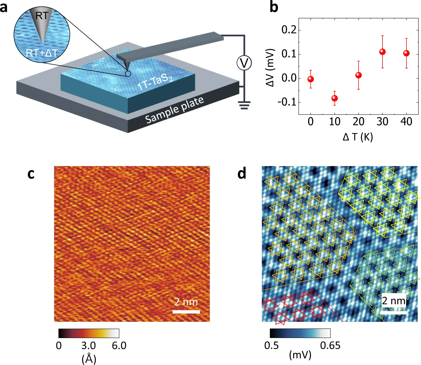
Fig. 1: SThEM of the nearly commensurate CDW phase in 1T-TaS2. a Schematic of the SThEM with 1T-TaS2. The temperature of the sample can be controlled from T=78 K to 450 K, and the tip is kept at room temperature in the SThEM. b Averaged thermopower (ΔV) as a function of temperature difference (ΔT). The ΔT is defined by Tsample-Ttip. Error bars represent standard deviations. c, d Topography c and SThEM images d of the nearly commensurate CDW phase in 1T-TaS2 with ΔT=30 K. Sulfur atoms and the SoD clusters are observed in both images. Besides the fine structures, four domains are visible in d. The sulfur atoms in the SoD are overlain to highlight the domain boundaries.
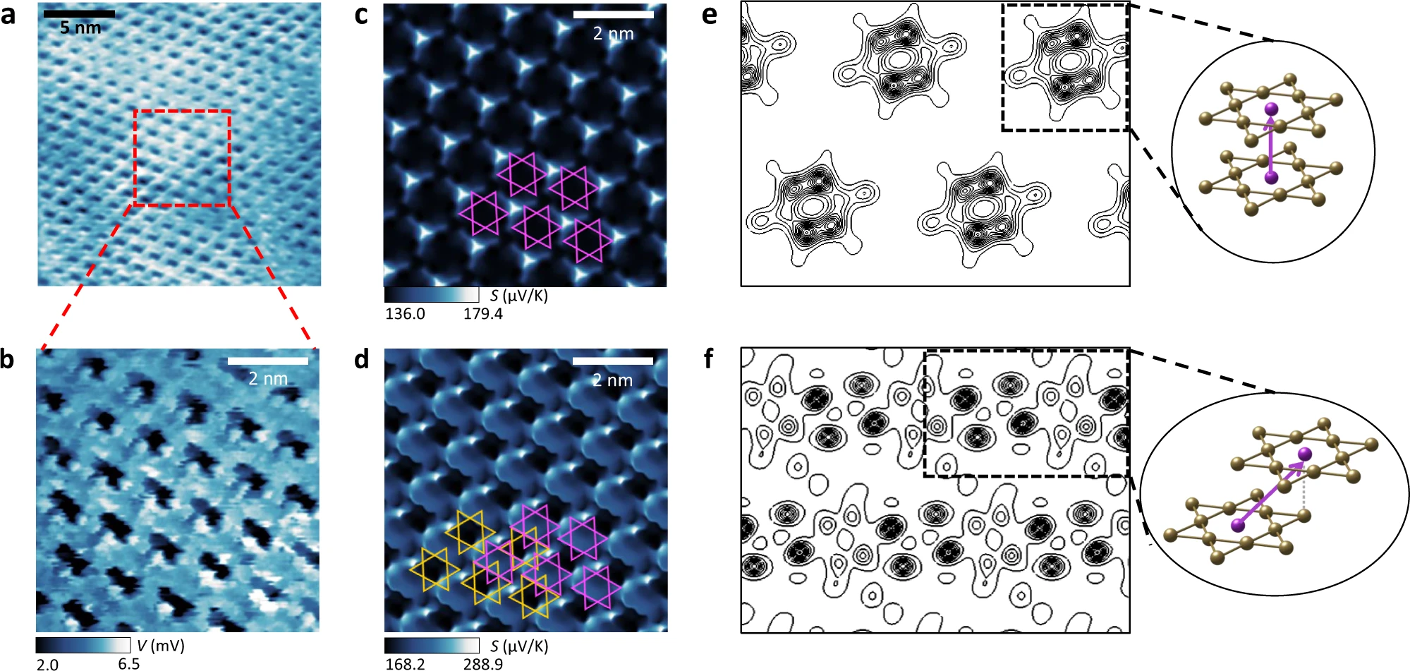
Fig. 2: SThEM of the Mott insulating and commensurate CDW phase in 1T-TaS2 with two stacking orders. a A SThEM image of the commensurate phase of 1T-TaS2 at Tsample=78 K. The Mott insulating gap and p-type nature of thermoelectricity appear as large and positive thermoelectric voltage signals. The ΔV varies up to 4 mV across the SoD clusters of atoms. b A magnified image of the SThEM of the commensurate CDW phase in 1T-TaS2, showing large ΔV fluctuation. c, d Theoretical scanning Seebeck profiles of A stacking c and L stacking d bilayer commensurate CDW phase in 1T-TaS2. The magenta and orange SoD in d denote the top and bottom layer CDW, respectively. e, f The valence electron densities of A stacking e and L stacking f bilayer in the middle of the two layers are shown with their atomic configuration for stacking. Only Ta atoms are displayed for clarity.
---
METHODS
Scanning thermoelectric microscopy (SThEM) measurement
We used an Omicron VT-SPM system for SThEM with a based pressure of 10−11 torr. The STM preamplifier was replaced by a high-impedance electrometer. All SThEM measurements were performed with a platinum-coated metallic cantilever. While the metallic tip was kept at room temperature, the 1T-TaS2 sample was heated by a PBN resistive heater or cooled by continuous-flow liquid nitrogen to generate a nominal temperature gradient ΔT at the tip-sample interface. The temperature gradient driven thermoelectric voltage was measured by a high-impedance electrometer in contact-AFM mode with a constant force feedback loop. The current flow in our SThEM is negligible with a high impedance (200 TΩ, Keithley 6517B) electrometer, which excludes the Joule heating effect at the junction. Moreover, the long retention time in our SThEM (5 ms) neglects the transient current during the heat transfer process at the junction within 1 ns time scale. The surface height variation and thermoelectric voltage mapping were obtained simultaneously, with a weak contact force range of 10−8 to 10−11 N.
Scanning tunneling microscopy (STM) and spectroscopy (STS)
All STM measurements were performed with a chemically etched tungsten tip using a Scienta Omicron VT-SPM system under a base pressure of 10−11 torr. For the low temperature measurement, the sample was cooled by a continuous liquid nitrogen cooling system. The STS was conducted on different CDW phases of the 1T-TaS2 sample, using a Stanford SR830 lock-in amplifier with a modulation voltage of 0.04 V and a frequency of 911.1 Hz.
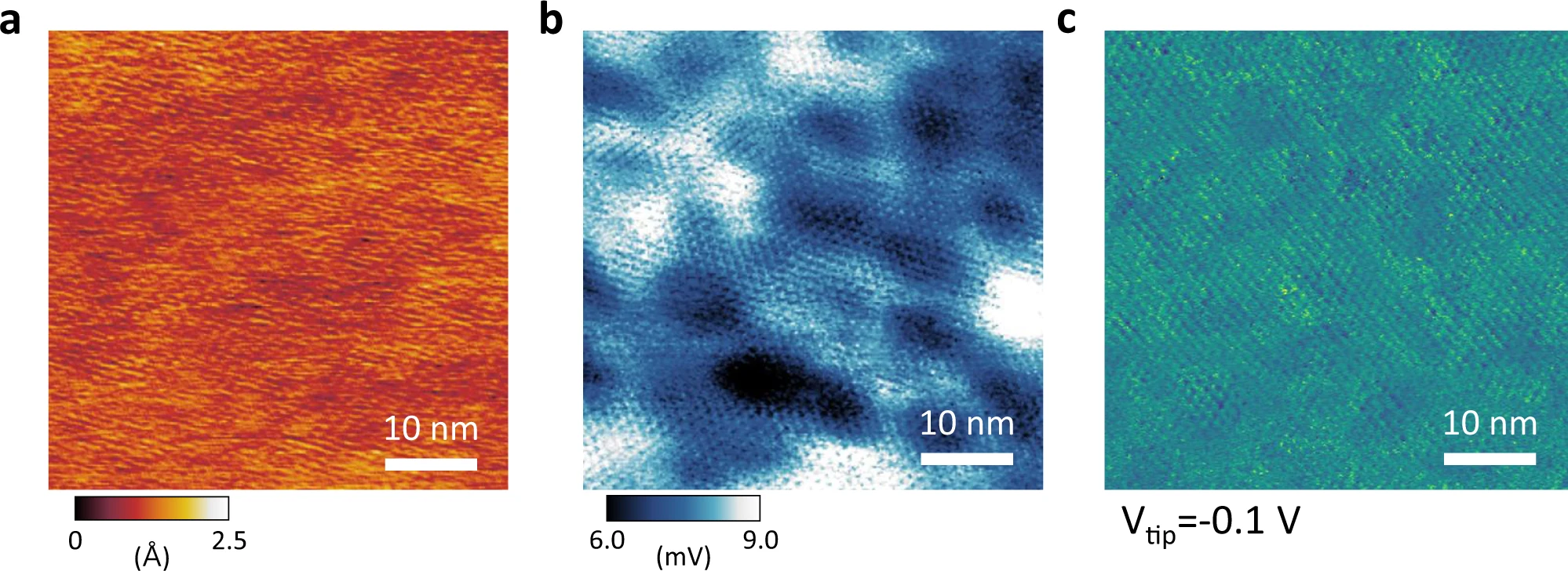
Fig. 3: Thermopower and charge puddles in the commensurate CDW phase in 1T-TaS2 by SThEM and STM. a, b Topography a and thermopower b images over a distance of 100 nm at Tsample=78 K. Despite the flat nature of the topography in a, the thermopower fluctuation shows a spatial variation of up to 3 mV, which is distinct from charge puddles in 1T-TaS2. The bulk single crystal of our 1T-TaS2 excludes the possibility of substrate effects for the ΔV fluctuation. c A dI/dV mapping image by STM with a tip voltage bias of Vtip=−0.1 V. Charge puddles near the Fermi level are observed with a subtle contrast, which suggests an additional origin for the large ΔV fluctuation in b.
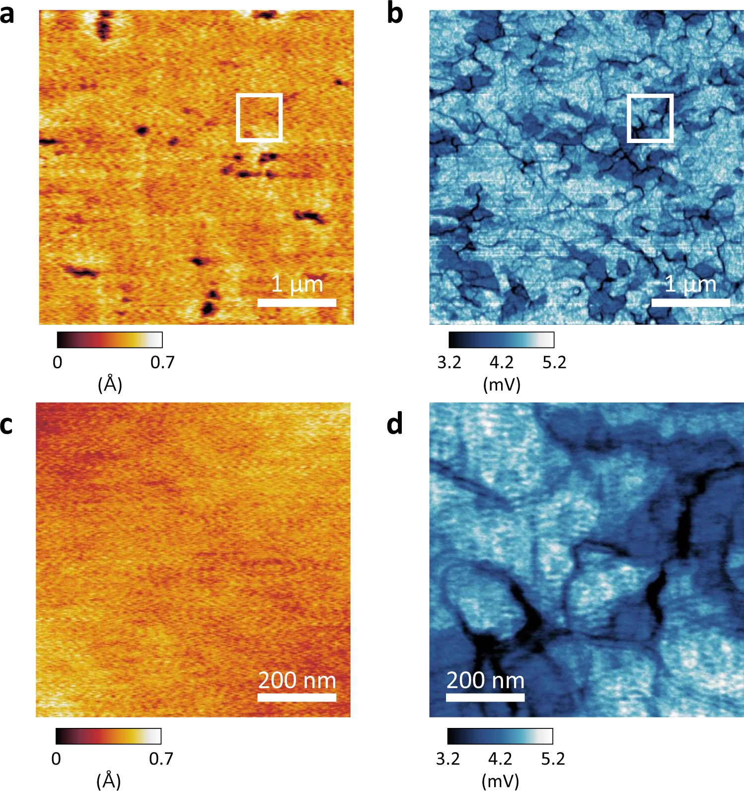
Fig. 4: Large-scale imaging of phonon puddles in the commensurate CDW phase of 1T-TaS2 by SThEM. a, b Topography a and thermopower b images over a distance of 4 μm at Tsample=78 K. Defect areas (pits and grain boundaries) in a exhibit lower thermopower in b. The thermopower image shows complex patterns that are not observed in the topography. c, d Magnified topography c and the corresponding thermopower d images highlighted by a white rectangle in a and b. While the flat area in c shows no structural disorder, the thermopower mapping in d reveals clear patterns with large contrast in ΔV, which originates from phonon puddles and the resulting effective ΔT at the junction between the tip and sample.
----
AUTHORS LIST
Dohyun Kim, Eui-Cheol Shin, Yongjoon Lee, Young Hee Lee, Mali Zhao, Yong-Hyun Kim & Heejun Yang
----
INSTITUTES LIST
- Department of Energy Science, Sungkyunkwan University, Suwon, Korea
- Dohyun Kim & Young Hee Lee
- Department of Physics, Korea Advanced Institute of Science and Technology (KAIST), Daejeon, Korea
- Eui-Cheol Shin, Yongjoon Lee, Yong-Hyun Kim & Heejun Yang
- Center for Integrated Nanostructure Physics (CINAP), Institute for Basic Science, Suwon, Korea
- Young Hee Lee
- Interdisciplinary Materials Research Center, College of Materials Science and Engineering, Tongji University, Shanghai, People’s Republic of China
- Mali Zhao
----
INSTITUTE WEBSITES
Department of Energy Science, Sungkyunkwan University
Quantum Energy Device Lab (QEDL)
----
JOURNAL AND LINK TO PUBLICATION
Nature Communications, https://www.nature.com/ncomms/
Publication: https://doi.org/10.1038/s41467-022-32226-y