µARPES & Electronic Alignment: Stay Focused, Save Time
 | © Scienta Omicron")
µARPES & Electronic Alignment advantages:
- Electronically shifts the analyser focal point in 3D to the emission spot
- Increases effective sample lifetime through fast and precise alignment
Note: You can upgrade your DA30-L with Electrostatic 3D focus adjustment.
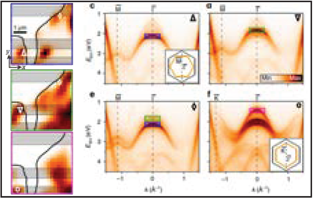
Figure 1: Local variations in the band structure of WS2 on a variable number of graphene layers resolved with nanoARPES (DA30-L). Intensity maps (a - c) are reconstructed based on specific regions of the band structure near the Γ point, indicated by coloured squares in (d - e), and highlight the local variation of electronic properties. The band structures of representative regions in (d - e) are extracted from regions indicated by the symbols in the intensity map. (Adapted from Ulstrup, S., Giusca, C.E., Miwa, J.A. et al. Nanoscale mapping of quasiparticle band alignment. Nat Commun 10, 3283 (2019). https://doi.org/10.1038/s41467- 019-11253-2, http://creativecommons.org/licenses/by/4.0/)
High quality µARPES data requires good control over the region of interest as well as an optimal alignment for ARPES measurement. The former is defined by the emission spot on the sample and the latter requires optimum alignment of the emission spot to the analyser for best deflection mode conditions. Without optimal alignment, measurement performance can be reduced (see Fig. 2 A and B). To optimise this alignment, common setups must mechanically change both the sample position and photon source to move the emission spot to the optimal measurement position of the analyser.
Inevitably this causes the emission spot to move on the sample and away from the region of interest. Changing the measurement conditions (Ek , Ep , lens mode) alters the electron optical conditions and requires small readjustments of the alignment.
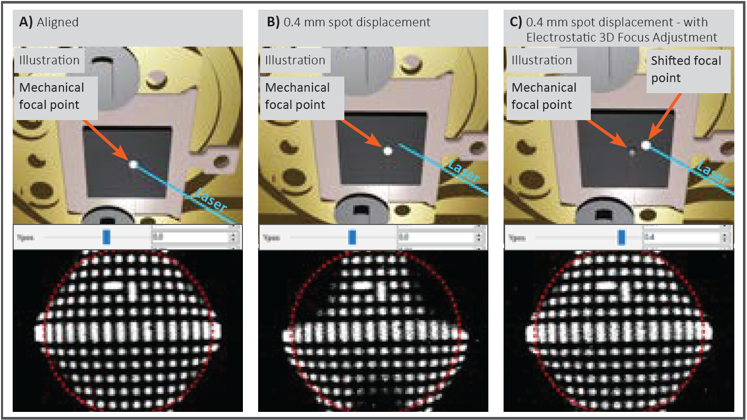
Figure 2: Electronic 3D Focus Adjustment results: A) shows a well-aligned situation with the analyser focal point and emission spot overlapping. The complete analyser acceptance angle, indicated by the red circle, is filled with accurate intensity. B) The 0.1 mm emission spot is misaligned by 0.4 mm. The corresponding measurement shows shadowing and asymmetry between the upper and lower half. C) Using Electrostatic 3D Focus Adjustment, the analyser focal point is easily shifted with a slider to the emission spot without any mechanical movement. The corresponding measurement shows the full accurate data expected for a well aligned situation. The grey point indicates the analyser mechanical focal point, without Electrostatic 3D Focus Adjustment.
Using electronic adjustment of the analyser lens to replace the imprecise mechanical adjustment of sample and photon source, achieves best deflection mode measurement performance (see Fig. 2 C) while ensuring the emission spot remains in the actual region of interest.
The DFS30 introduces this groundbreaking electronic adjustment of the analyser lens to provide a significantly improved workflow, speed, and reproducibility when optimizing experimental conditions.