Molecular Beam Epitaxial (MBE) Growth of Topological Materials
Topological materials are a significant focus in today‘s condensed matter physics, as pointed out in the excellent perspective article recently compiled by Matthew Brahlek et al [1]. The novel physics arises from the special electronic band structure, based on band inversion. The novel states only determine the properties of the material when the Fermi level is positioned at a particular location in the band structure. For Topological Insulators (TIs) the Fermi level must be close to the 2D Dirac point, as shown schematically in Figure 1a (EF,ideal). Likewise, in Dirac and Weyl semimetals the Fermi level should be close to the 3D Dirac or Weyl point. The positioning of the Fermi level requires a high level of control over the growth process.
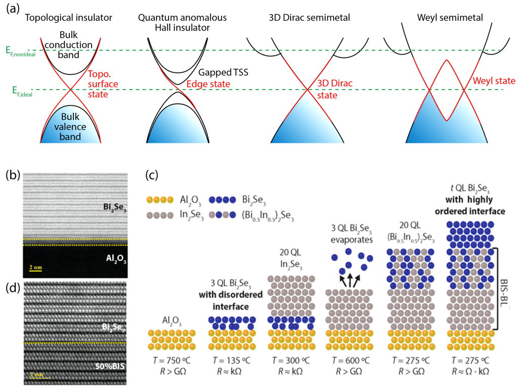
Figure 1. (a) Schematics of topological band structures for selected material classes. (b) TEM image of Bi2Se3 on Al2O3, showing increased defect density in the interface region. (c) Schematic of the virtual substrate method. (d) TEM image of the highly ordered interface between Bi2Se3 and the virtual substrate. Reprinted from Brahlek et al., J. Appl. Phys. 128, 210902 (2020), with the permission of AIP Publishing. Reprinted (adapted) with permission from Koirala et al., Nano Lett. 15, 8245 (2015). © 2015 American Chemical Society.
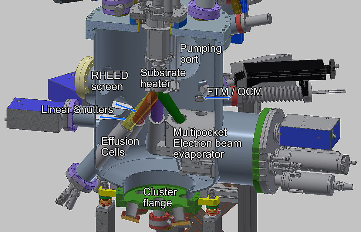
Molecular Beam Epitaxy (MBE) is the ultimate method for well-controlled UHV growth with beams of atoms or molecules of dissimilar chemical species converging onto a substrate crystal (see Figure 2). At the substrate surface, the impinging atoms may diffuse, adsorb or desorb. For each material system, there is an optimum substrate temperature for growth, balancing surface diffusion and desorption. Optimisation of these growth conditions is moderated by understanding and minimising defects in the new material.
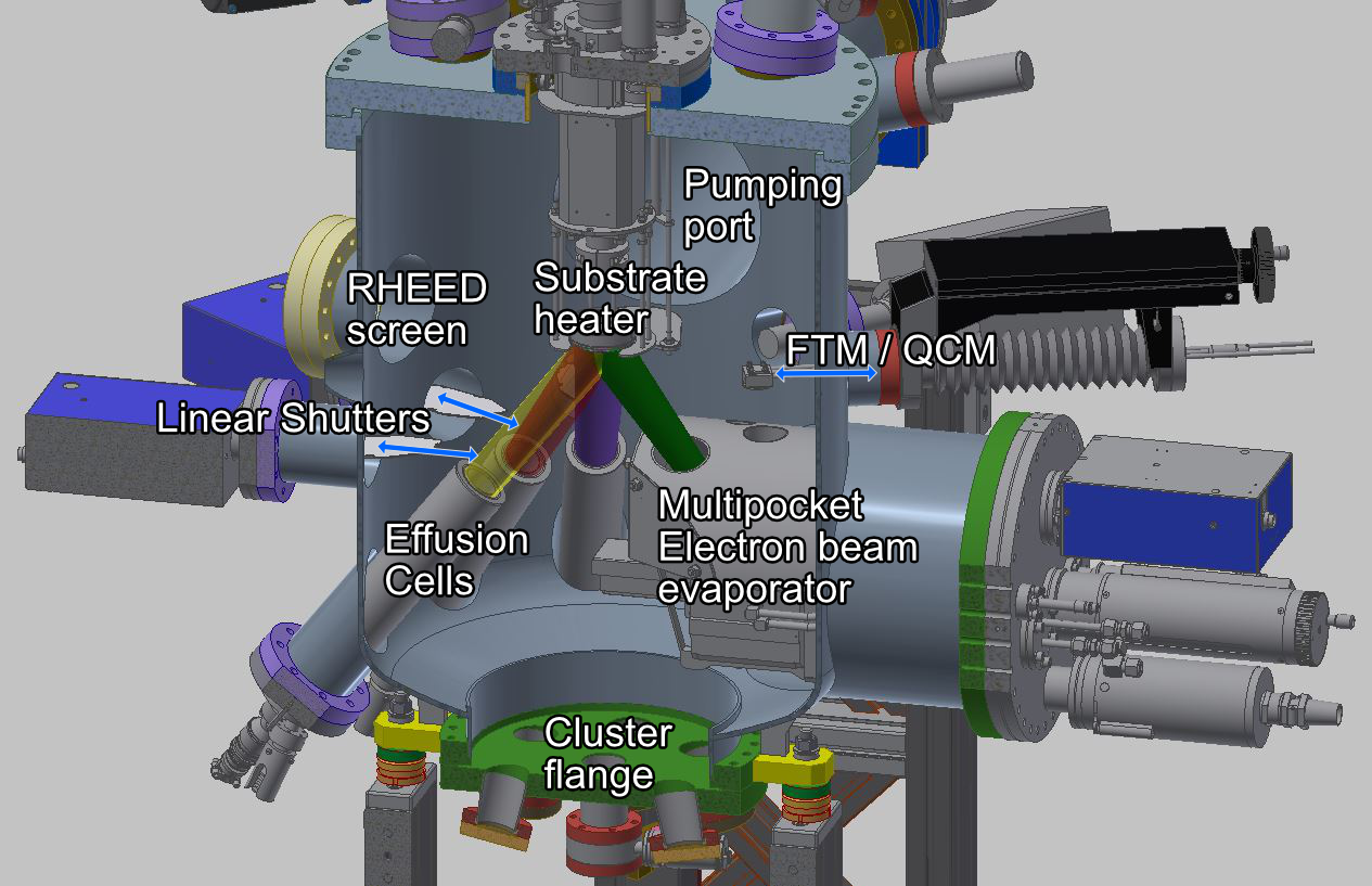
Figure 2. Schematic of the Scienta Omicron EVO-50 MBE chamber as delivered to the authors of the article [1]. The liquid nitrogen cryopanel is not displayed.
TI’s and their associated band structures are highly sensitive to defects. If defect density is too high, the material loses its exceptional properties, as it goes over to a trivial phase. A major source of defects for thin films are interfaces. A known defect mitigation strategy, borrowed from traditional semiconductor heterostructure growth, is to employ a “virtual substrate” [2]. In this process, a buffer layer that is epitaxially and chemically matched to the active material is grown between the substrate and TI. An example of the application of the virtual substrate method is shown for a tetradymite TI in Figure 1c. The reduction of interfacial defects by the addition of In2Se3 and (Bi0.5In0.5)2Se3 buffer layers led to a reduction in charge carrier density and an increase in mobility for Bi2Se3 on Al2O3 substrate [2].
Refining the growth process requires a thorough understanding of the inherent properties of the desired synthesised sample, may it be intrinsic topological materials or heterostructures. Angle-Resolved Photoemission Spectroscopy (ARPES) has been proven to be a powerful tool for directly probing the surface band structure. Another technique that is commonly used for studying surface topography and information about the electronic structure on a specific spot is Scanning Tunnelling Microscopy (STM). As many topological materials degrade rapidly in air, the use of interconnected MBE-surface analysis systems is an indispensable approach for probing the inherent properties of the synthesised TIs. The in-situ combination of growth and analysis in a Materials Innovation Platform (MIP) is a time-efficient route to reveal signatures of non-trivial phases, e.g. 2D topological superconductivity. Scienta Omicron is proud to contribute with integrated MBE and surface analysis instruments to the investigation and development of topological materials.