Deep-ultraviolet transparent conducting SrSnO3 via heterostructure design
Result of the Month
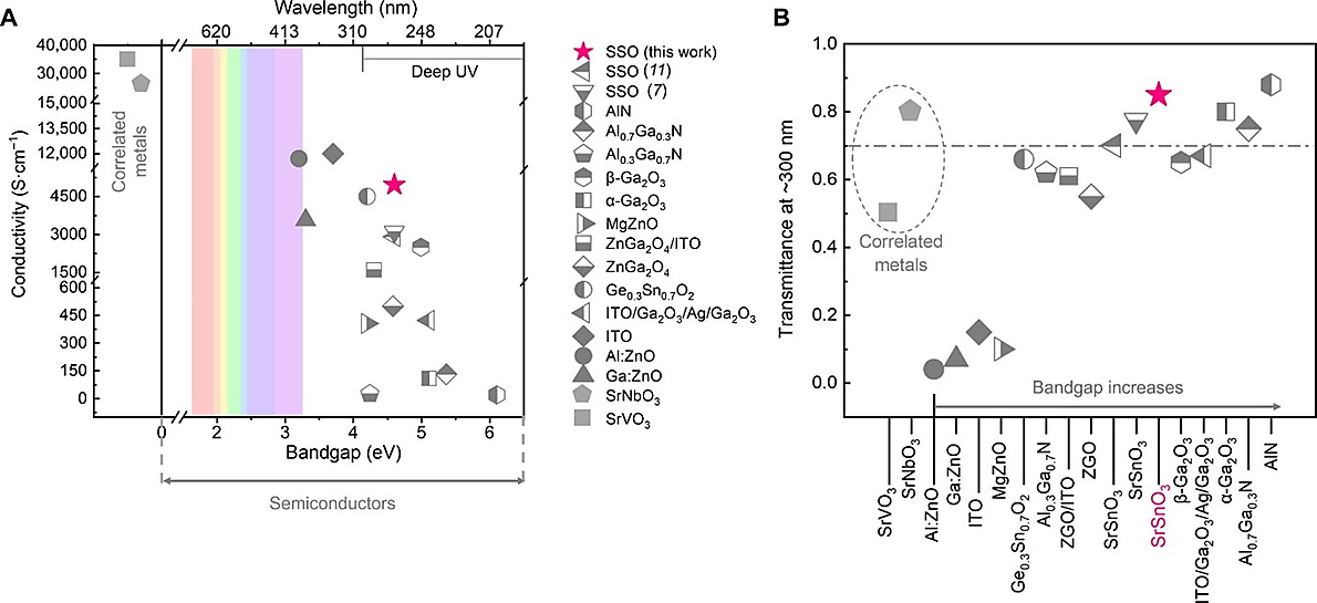

Comparison of the conductivity and optical transmittance of transparent conductors. (A) Room-temperature electrical conductivity of selected transparent conducting materials as a function of the bandgap along with the conductivity of correlated metals SrNbO3 and SrVO3 thin films. The effective conductivity of 4 nm SrSnO3/19 nm La: SrSnO3/GdScO3 (110) is included for comparison. (B) Optical transmittance at a wavelength ~300 nm for films outlined in (A). The thickness of the films: SrVO3 (4 nm), Al: ZnO (280 nm), Ga: ZnO (180 nm), ITO (1000 nm), SrNbO3 (10 nm), MgZnO (500 nm), Ge0.3Sn0.7O2 (200 nm), Al0.3Ga0.7N (390 nm), ZnGa2O4/ITO (200 nm/25 nm), ZnGa2O4 (single crystal), SrSnO3 (112 nm), SrSnO3 (120 nm), SrSnO3 (3 nm undoped/13 nm doped), β-Ga2O3 (200 nm), ITO/Ga2O3/Ag/Ga2O3 (10 nm/15 nm/7 nm/15 nm), α-Ga2O3 (600 nm), Al0.7Ga0.3N (518 nm), AlN (300 nm).
Ultra-wide-bandgap (UWBG) semiconducting oxides are becoming pivotal in sustainable technologies due to their promising applications in next-generation high-power electronics and deep-ultraviolet (DUV) optoelectronics. This entails the need for a UWBG semiconductor that can effectively accommodate robust doping with tunable carrier concentrations, and high electrical conductivity and mobility. We have employed a thin heterostructure comprising 4 nm SrSnO3/19 nm La-doped SrSnO3/GdScO3 (110) grown by hybrid molecular beam epitaxy (MBE). We utilize the heterostructure design to effectively separate electrons in SrSnO3 from dopants due to the Fermi level equilibration and charge transfer at the interface. We also apply electrostatic gating with ion gels to further modify electron densities. Both methods allow us to achieve phonon-limited transport behavior in strain-stabilized tetragonal SrSnO3 and lead to a modulation of carrier density from 1018 cm-3 to 1020 cm-3, with room-temperature mobilities ranging from 40 to 140 cm2V-1s-1. The phonon-limited mobility, calculated from first principles, closely matches experimental results, suggesting that room-temperature mobility could be further increased with higher electron density. Additionally, we have demonstrated that both high electrical conductivity (over over 4,900 S cm-1) and high optical transmittance (85% at a 300 nm wavelength) can be achieved with the heterostructure design as shown in the image 1, which highlights the potential of the heterostructure design for transparent UWBG semiconductor applications especially in deep-ultraviolet regime.
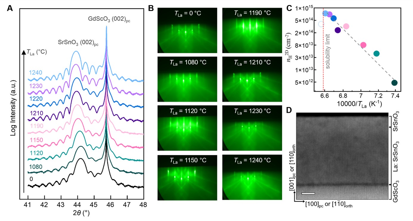
Characterization of SrSnO3 thin films.
(A) High resolution X-ray diffraction 2θ-ω couple scan of 4 nm SrSnO3/19 nm La: SrSnO3/GdScO3 (110) thin films with different La cell temperatures. (B) Reflection high-energy electron diffraction (RHEED) patterns of these thin films with the beam pointing along the [ ]orth direction. (C) Measured 2D carrier concentrations nH2D as a function of inverse of La cell temperatures 10000/TLa. (D) Atomic resolution HAADF-STEM cross-sectional image of a representative 4 nm SrSnO3/19 nm La: SrSnO3/GdScO3 (110) substrate. Scale bar = 5 nm. The image is low-pass filtered.
Using the EVO-50 UHV oxide MBE system equipped with a radio-frequency oxygen plasma system, custom vapor inlet system for the metal-organic Sn source, effusion cells for elemental Sr and La sources, beam flux monitor and RHEED, we are able to grow high-quality SrSnO3/La-doped SrSnO3 thin films with precise control of the La doping density and the thickness of each layer, which allows us to study the electrical transport properties of the resulting heterostructure.