
ZyVector
STM Control System for Atomically Precise Lithography
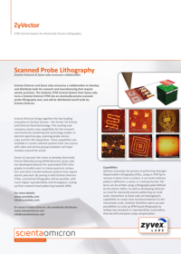
SPM STM HDL Manipulation Nanolithography
- Digital Lithography
- Sub-nm pixel
- Vector Writing, aligned to Atomic Lattice
- Multiple beam widths
- Built-in Metrology
- Automation and Scripting
- Automated Imaging, Moving and Writing
- Vector or Bitmap pattern input modes
- Precise Tip Positioning and Motion
- Real-time Creep Correction
- Fiducial recognition and alignment
- Pattern alignment to Lattice
ZyVector is an STM control system which converts a scanning tunneling microscope into an automated STM lithography system. The system is controlled through our software package, Scanz, which allows for automation of almost every task, including Digital Vector Lithography. The software drives a 20-bit digital control box to handle the real-time control tasks such as the STM feedback loop and the creep and hysteresis correction which allows for precise tip positioning. This drives high-voltage amplifiers to drive the STM piezo scanner. ZyVector is designed to connect to Scienta Omicron UHV STMs using the standard Scienta Omicron STM cabling. It can also be adapted to run other STM systems.
More Information
Digital Vector Lithography

Unlike conventional optical or e-beam lithography, ZyVector takes into account the atomic structure of the surface. Writing is done as vectors, moving along the surface lattice vectors, with a standard pixel size of 2 dimers on a single dimer row. Using different settings of voltage and current, multiple beam widths are available, from one pixel wide up to several nm, to optimize write time for larger patterns. There is no partial exposure; either a H atom is removed, or it is not. Proximity effects also do not exist here.
One final advantage over conventional e-beam lithography is the ability to image nondestructively with the same tip as used for writing. Thus the surface can be imaged prior to writing, allowing alignment to fiducial marks or areas of previous patterning. After writing, the quality of the lithography can be checked, enabling some error correction.
Finally, the written pattern can be imaged with atomic precision, so that developed nanostructures can be referred back to the original pattern.
Automation and Scripting

ZyVector enables automation and user scripting of almost every part of the software, including both imaging, and writing. Patterns to be written can be input via the user interface, or in a script as a list of vectors or as a bitmap, which is converted into write vectors by ZyVector, with one bitmap pixel corresponding to the 0.768 nm pixel defined by the Si(001) lattice.
Precise Tip Positioning and Motion
Piezoelectric elements used in commercial STM systems suffer from time-dependent errors called creep. These creep errors are corrected in real time in our control system, so that STM images are undistorted, and lithography vectors follow their desired path. The system can also automatically find fiducial marks on the surface, and align to them, so that different parts of a pattern are kept in registry with each other.
Downloads
ZyVector: STM Control System for Lithography
Scienta Omicron and Zyvex Labs announce a collaboration to develop and distribute tools for research and manufacturing that require atomic precision. The ZyVector STM Control System from Zyvex Labs turns a Scienta Omicron STM into an atomically-precise scanned probe lithography tool, and will be distributed world-wide by Scienta Omicron.