
Engineering quantum wires states on hydrogen terminated silicon for atom scale circuitry
Result of the Month
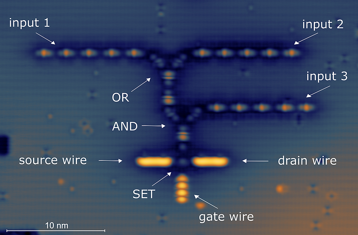
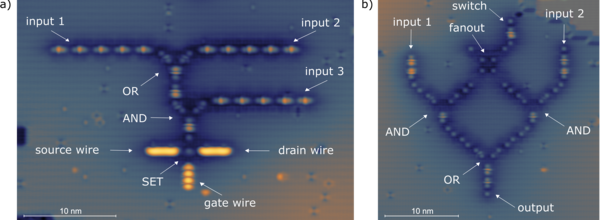
Two prototype atomic silicon integrated circuits are shown to demonstrate current capabilities to fabricate complex error-free silicon DB structures using STM-based HL on an H- terminated surface. (a) 1.3 V, 50 pA STM image of a three-input combination OR gate and AND gate with atom-defined SET readout formed out of 69 DBs. (b) 1.3 V, 50 pA STM image of a two-input multiplexing DB circuit made of several gates and a fanout formed out of 56 DBs. Both circuit layouts were made using gate designs from binary atomic silicon logic and were based on modelling and simulation software for silicon DB logic systems.
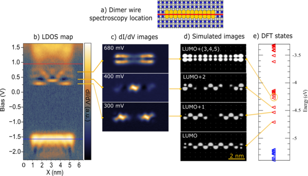
Characterizing a 12-dimer long wire using dI/dV spectroscopy, imaging, and DFT simulations.
(a) An atom diagram indicating the location of the dI/dV spectroscopy with respect to the wire. (b) A 1D dI/dV map taken over the 12-dimer long wire using a 1.8 V and 50 pA tip set point over H−Si. Apparent band edges are shown in blue (VB) and red (CB). (c) Constant height dI/dV images of the wire from the same set point. Energies were chosen to correspond to states shown in (b). (d) Simulated dI/dV images for the first several states in the band gap. (e) A calculated energy level diagram for the dimer wire showing the manifold of filled (blue) and empty (red) states for the wire, analogous to the experimental data in (b).
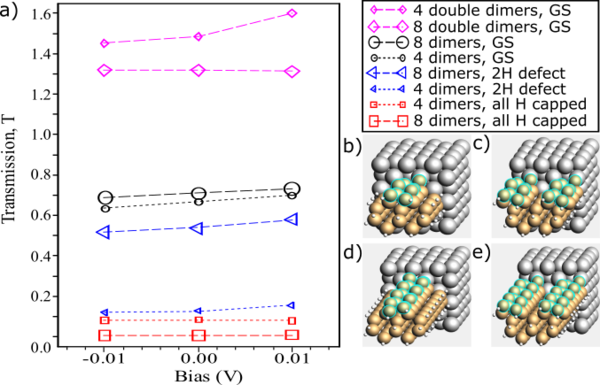
Quantum transport calculation through 4- and 8-long dimer wires on Si nanoclusters sandwiched between metal electrodes, predicted using the NEGF-DFT method in the limit of low to zero bias. (a) The compiled values of the transmission function as a function of bias for various wire lengths and types, indicated in the legend. GS stands for the “ground state” configuration of the wire. The lines connecting the symbols are just a visualization aid. The remaining panels indicate the ground-state geometries used in the calculations of four wire types: (b) 4-long single dimer wire; (c) 4-long double dimer wire; (d) 8-long single-dimer wire; (e) 8-long double dimer wire. Si atoms are depicted in yellow, H atoms in white, Ag atoms in gray, with the Si atoms hosting DBs being highlighted in light green. Only the far-side electrode is shown for clarity.