Accelerating Materials Innovation
Electron Spectroscopy

Scanning Probe Microscopy

Thin Film Deposition

Result of the Month (ROM), July 2026
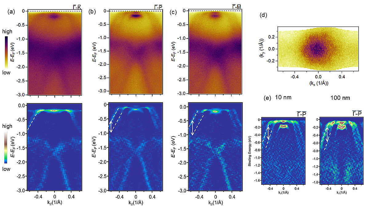
Altermagnetic Band Splitting in 10 nm Epitaxial CrSb Thin Films
Altermagnets are a newly identified family of collinear antiferromagnets with a momentum-dependent spin-split band structure of non-relativistic origin, derived from spin-group symmetry-protected crystal structures. Among candidate altermagnets, CrSb is attractive for potential applications because of a large spin-splitting near the Fermi level and a high Néel transition temperature of around 700 K. Molecular beam epitaxy is used to synthesize CrSb (0001) thin films with thicknesses ranging from 10 to 100 nm. Structural characterization, using reflection high energy electron diffraction, scanning transmission electron microscopy, and X-ray diffraction, demonstrates the growth of epitaxial films with good crystallinity. Polarized neutron reflectometry shows the absence of any net magnetization, consistent with antiferromagnetic order. In vacuo angle resolved photoemission spectroscopy (ARPES) measurements probe the band structure in a previously unexplored regime of film thickness, down to 10 nm. These ARPES measurements show a bulk-type, 3D momentum-dependent band splitting of up to 0.7 eV with g-wave symmetry, consistent with that seen in prior studies of bulk single crystals. The distinct altermagnetic band structure required for potential spin-transport applications survives down to the ∼10 nm thin film limit at room temperature.
Latest news
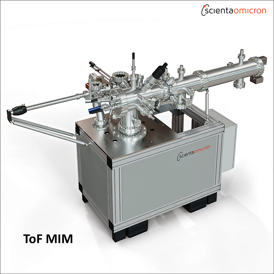
Introducing ToF MIM
The global electronic band structure and its dynamics are of great interest in quantum materials. Scienta Omicron’s Time-of-Flight Momentum and Imaging Microscope (ToF MIM) is an efficient tool to characterise global electronic band structure and microstructure at once. It is ideally suited to study ultrafast electron dynamics in pump-probe experiments using ultrashort laser pulses.
Sample Manipulators

Open and Closed Cycle Sample Manipulators
When aiming at high experimental energy resolution for ARPES measurement, it is crucial to achieve ultra-low sample temperatures to quench thermal broadening. This is possible with state-of-the-art cryo manipulators reaching sample temperatures from < 3.5 K and featuring up to 6 fully motorized axes for a large range of movements. The manipulators are available as open and closed cycle. Open cycle manipulators reach lower temperature specifications and are rapidly cooled down from room temperature to 10 K in 15 min. The low He consumption below 1 l/h at ultimate temperature and the possibility to operate with liquid nitrogen at higher temperatures ensure a low operating cost. Closed cycle manipulators have no He consumption providing unlimited holding time.
Service Upgrade
PEAK Slit Control
Optimal analyser settings with remote control
In photoelectron spectroscopy measurements, there is always a trade-off between signal intensity and resolution. Optimising this balance is the key to obtaining smooth and sharp spectra within the shortest time possible. For hemispherical analysers, this trade-off is controlled by the selected entrance slit and pass energy.
PEAK Slit Control replaces manual slit changes at the analyser with a motorised and software-controlled slit. With the control of all analyser settings, easy and quick optimisation of signal intensity versus resolution is possible.
About Us
Scienta Omicron is a leading innovator in Surface Science and Nanotechnology. At our technology centres in Uppsala, Sweden and Taunusstein, Germany we develop and produce high-tech instruments. Our instruments support top researchers globally and are serviced by our four regional hubs in USA, China, Japan and Germany.
We provide state of the art instruments in Electron Spectroscopy, Scanning Probe Microscopy and Thin Film Deposition. Focusing on the race for new unique materials and solutions, in areas like – smarter batteries, next generation electronics, quantum technologies, solar energy, intelligent sensors and advanced materials, Scienta Omicron enables development of tomorrow´s materials.
THE SCIENTA GROUP: One Group, Two Leading Brands

Since 1983 the combined companies, including Scienta Omicron and Scienta Envinet (former Scienta Sensor Systems and Envinet GmbH respectively) that make up the Scienta Scientific Group have been leading the development of ultra high vacuum research and analysis equipment in the fields of Surface Science, Material Physics, UHV technology and Radiation Detection, resulting in scientific breakthroughs, Nobel Prizes and outstanding industrial equipment.